2026
|
Ikshvaku Shyam; Raj Singh; Mangababu Akkanaboina; A. M. Sonawane; Muthu Satheeshkumar; Amrita Majumder; Ekta; Janhavi Jayawant Khunte; Akash Khaire; Kenji Watanabe; Takashi Taniguchi; Gopalan Rajaraman; S. S. Dahiwale; Anshuman Kumar Hexagonal Boron Nitride Spin Defects for Quantum Photonics: Annealing-Free Generation by Krypton Ion Implantation Journal Article In: arXiv preprint, vol. arXiv:2606.23334 , 2026. @article{arXiv:2606.23334,
title = {Hexagonal Boron Nitride Spin Defects for Quantum Photonics: Annealing-Free Generation by Krypton Ion Implantation},
author = {Ikshvaku Shyam and Raj Singh and Mangababu Akkanaboina and A. M. Sonawane and Muthu Satheeshkumar and Amrita Majumder and Ekta and Janhavi Jayawant Khunte and Akash Khaire and Kenji Watanabe and Takashi Taniguchi and Gopalan Rajaraman and S. S. Dahiwale and Anshuman Kumar},
url = {https://doi.org/10.48550/arXiv.2606.23334},
doi = {10.48550/arXiv.2606.23334},
year = {2026},
date = {2026-06-22},
journal = {arXiv preprint},
volume = {arXiv:2606.23334 },
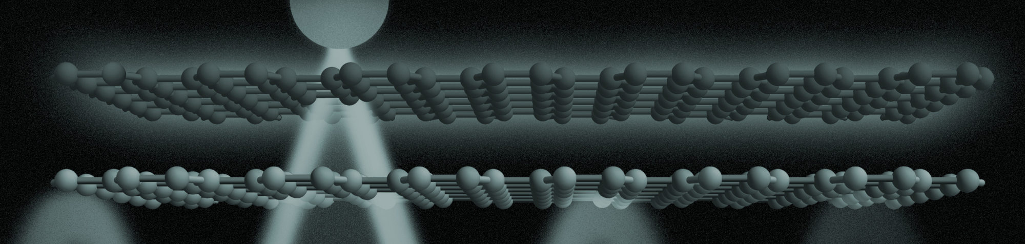
abstract = {Controlled, reproducible generation of luminescent defect centres in hBN remains a key challenge for scalable quantum-photonic technologies. Here, we report Kr ion implantation as a tunable, annealing-free, and chemically inert route to room-temperature near-infrared luminescent spin defects in hBN, requiring no pre- or post-implantation annealing. SRIM Monte Carlo simulations were used to optimise the parameters for 40 keV Kr irradiation of hBN flakes. The implanted samples exhibit a stable near-infrared photoluminescence (PL) band centred at 830 nm whose intensity increases with implantation fluence over -ions/cm. Temperature-dependent PL measurements (20-300 K) reveal a linewidth broadening well described by a dependence, consistent with acoustic-phonon-mediated dephasing. Raman spectra show the characteristic mode of pristine hBN at 1366 cm alongside an implantation-induced defect feature at 1295 cm, confirming irradiation-induced lattice disorder. Electron paramagnetic resonance (EPR) measurements reveal a paramagnetic centre with a -factor of 2.003, and density functional theory (DFT) calculations indicate that a spatially separated - donor-acceptor pair complex is a viable origin of the observed optical and magnetic signatures. Overall, Kr implantation offers an effective, annealing-free, and scalable platform for generating stable room-temperature luminescent defects, providing a promising route toward quantum photonics.},
keywords = {},
pubstate = {published},
tppubtype = {article}
}
Controlled, reproducible generation of luminescent defect centres in hBN remains a key challenge for scalable quantum-photonic technologies. Here, we report Kr ion implantation as a tunable, annealing-free, and chemically inert route to room-temperature near-infrared luminescent spin defects in hBN, requiring no pre- or post-implantation annealing. SRIM Monte Carlo simulations were used to optimise the parameters for 40 keV Kr irradiation of hBN flakes. The implanted samples exhibit a stable near-infrared photoluminescence (PL) band centred at 830 nm whose intensity increases with implantation fluence over -ions/cm. Temperature-dependent PL measurements (20-300 K) reveal a linewidth broadening well described by a dependence, consistent with acoustic-phonon-mediated dephasing. Raman spectra show the characteristic mode of pristine hBN at 1366 cm alongside an implantation-induced defect feature at 1295 cm, confirming irradiation-induced lattice disorder. Electron paramagnetic resonance (EPR) measurements reveal a paramagnetic centre with a -factor of 2.003, and density functional theory (DFT) calculations indicate that a spatially separated - donor-acceptor pair complex is a viable origin of the observed optical and magnetic signatures. Overall, Kr implantation offers an effective, annealing-free, and scalable platform for generating stable room-temperature luminescent defects, providing a promising route toward quantum photonics. | 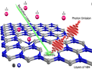 |
Amrita Majumder; Janhavi Khunte; Ikshvaku Shyam; Rohit Kumar; Anshuman Kumar Deterministic single-photon sources in hexagonal boron nitride with electron-dose-tuned purity and reversible thermal quenching Journal Article In: arXiv preprint, vol. arXiv:2606.16977, 2026. @article{arXiv:2606.16977,
title = {Deterministic single-photon sources in hexagonal boron nitride with electron-dose-tuned purity and reversible thermal quenching},
author = {Amrita Majumder and Janhavi Khunte and Ikshvaku Shyam and Rohit Kumar and Anshuman Kumar},
url = {https://doi.org/10.48550/arXiv.2606.16977},
doi = {10.48550/arXiv.2606.16977},
year = {2026},
date = {2026-06-16},
journal = {arXiv preprint},
volume = {arXiv:2606.16977},
abstract = {Electron-beam irradiation is an established route to create site-controlled, room-temperature single-photon emitters (SPEs) in hexagonal boron nitride (hBN), but two aspects remain underexplored: how the electron dose governs the properties of the resulting single emitters, and how the emission behaves when the host is heated above room temperature. Here, we create emitters deterministically with a focused electron beam and confirm single-photon emission across three independent flakes through second order photon correlation measurements. We map the single-emitter response (yield, spectrum, lifetime, and photon purity) as a function of electron dose, identifying an optimal window for high-purity single emitters. Consistent with recent cryogenic studies, we assign the bright room-temperature feature near 575 nm to the phonon sideband (PSB) of a green--yellow emitter whose zero-phonon line (ZPL) lies near 548 nm. Temperature-dependent photoluminescence measured in situ under real-time from room temperature to 300 degrees C reveals a thermal quenching that is fully reversible upon cooling, in contrast to the irreversible annealing-induced degradation reported elsewhere, indicating that transient heating does not permanently damage the centers. These results add quantitative dose control and above-room-temperature operation to the toolbox for deterministic hBN quantum-light sources.},
keywords = {},
pubstate = {published},
tppubtype = {article}
}
Electron-beam irradiation is an established route to create site-controlled, room-temperature single-photon emitters (SPEs) in hexagonal boron nitride (hBN), but two aspects remain underexplored: how the electron dose governs the properties of the resulting single emitters, and how the emission behaves when the host is heated above room temperature. Here, we create emitters deterministically with a focused electron beam and confirm single-photon emission across three independent flakes through second order photon correlation measurements. We map the single-emitter response (yield, spectrum, lifetime, and photon purity) as a function of electron dose, identifying an optimal window for high-purity single emitters. Consistent with recent cryogenic studies, we assign the bright room-temperature feature near 575 nm to the phonon sideband (PSB) of a green--yellow emitter whose zero-phonon line (ZPL) lies near 548 nm. Temperature-dependent photoluminescence measured in situ under real-time from room temperature to 300 degrees C reveals a thermal quenching that is fully reversible upon cooling, in contrast to the irreversible annealing-induced degradation reported elsewhere, indicating that transient heating does not permanently damage the centers. These results add quantitative dose control and above-room-temperature operation to the toolbox for deterministic hBN quantum-light sources. | 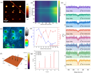 |
Mangababu Akkanaboina, Rohit Kumar Brijesh Kumar; Hrushikesh Gawali; Parul Sharma; Ikshvaku Shyam; Anshuman Kumar Deterministic Single-Photon Emitter Arrays in Hexagonal Boron Nitride by Carbon-Assisted Focused Ion Beam Engineering Journal Article In: arXiv preprint, vol. arXiv:2606.12304 , 2026. @article{arXiv:2606.12304,
title = {Deterministic Single-Photon Emitter Arrays in Hexagonal Boron Nitride by Carbon-Assisted Focused Ion Beam Engineering},
author = {Mangababu Akkanaboina, Rohit Kumar Brijesh Kumar and Hrushikesh Gawali and Parul Sharma and Ikshvaku Shyam and Anshuman Kumar},
url = {https://doi.org/10.48550/arXiv.2606.12304},
doi = {10.48550/arXiv.2606.12304},
year = {2026},
date = {2026-06-11},
journal = {arXiv preprint},
volume = {arXiv:2606.12304 },
abstract = {The realization of on-chip photonic circuits requires scalable and deterministic single-photon emitters (SPEs) at room temperature, which remain a challenge in van der Waals materials. In this work, we report a novel three-step fabrication process for the generation of spatially controlled SPE arrays in hexagonal boron nitride (hBN). The process comprises site-selective gallium (Ga) focused ion beam milling, nanoscale conformal carbon deposition over the patterned regions, and subsequent thermal annealing. The synergistic combination of these steps resulted in a site-correlated emitter yield of 89 percent across 100 fabrication sites. Second-order autocorrelation measurements revealed pronounced three-level emitter dynamics where the best emitters exhibited high purity (0.15). To the best of our knowledge, this is the first lithography-free, direct-write approach combining Ga-ion milling, selective carbon engineering, and thermal annealing to deterministically generate hBN SPEs. The reproducibility of the method is validated across multiple independently fabricated samples. These results establish a scalable, lithography-free pathway toward on-demand SPE arrays relevant to integrated quantum photonics.},
keywords = {},
pubstate = {published},
tppubtype = {article}
}
The realization of on-chip photonic circuits requires scalable and deterministic single-photon emitters (SPEs) at room temperature, which remain a challenge in van der Waals materials. In this work, we report a novel three-step fabrication process for the generation of spatially controlled SPE arrays in hexagonal boron nitride (hBN). The process comprises site-selective gallium (Ga) focused ion beam milling, nanoscale conformal carbon deposition over the patterned regions, and subsequent thermal annealing. The synergistic combination of these steps resulted in a site-correlated emitter yield of 89 percent across 100 fabrication sites. Second-order autocorrelation measurements revealed pronounced three-level emitter dynamics where the best emitters exhibited high purity (0.15). To the best of our knowledge, this is the first lithography-free, direct-write approach combining Ga-ion milling, selective carbon engineering, and thermal annealing to deterministically generate hBN SPEs. The reproducibility of the method is validated across multiple independently fabricated samples. These results establish a scalable, lithography-free pathway toward on-demand SPE arrays relevant to integrated quantum photonics. | 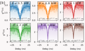 |
Anushka Kumari; Anushree Khisti; Abhinav Choube; Devansh Satra; Srivatsa Murali; Anshuman Kumar Multimodal Optical Feature Extraction with a Free-Space Photonic Extreme Learning Machine Journal Article In: arXiv preprint, vol. 2605.29043 , 2026. @article{pelm,
title = {Multimodal Optical Feature Extraction with a Free-Space Photonic Extreme Learning Machine},
author = {Anushka Kumari and Anushree Khisti and Abhinav Choube and Devansh Satra and Srivatsa Murali and Anshuman Kumar},
url = {https://doi.org/10.48550/arXiv.2605.29043},
doi = {10.48550/arXiv.2605.29043},
year = {2026},
date = {2026-05-29},
urldate = {2026-05-29},
journal = {arXiv preprint},
volume = {2605.29043 },
abstract = {Photonic extreme learning machines (PELMs) replace a digitally trained hidden layer by a fixed optical transformation, allowing a high dimensional feature map to be generated by physical propagation while only the final readout is learned. Existing free-space PELM demonstrations have established this principle for image and tabular benchmarks, but a unified multimodal optical feature extractor spanning structurally different data types has remained largely undeveloped. Here we demonstrate a single free-space PELM platform for image, audio derived, binary tabular, and regression tasks using phase only SLM encoding, Fourier like free space propagation, and camera intensity detection.},
keywords = {},
pubstate = {published},
tppubtype = {article}
}
Photonic extreme learning machines (PELMs) replace a digitally trained hidden layer by a fixed optical transformation, allowing a high dimensional feature map to be generated by physical propagation while only the final readout is learned. Existing free-space PELM demonstrations have established this principle for image and tabular benchmarks, but a unified multimodal optical feature extractor spanning structurally different data types has remained largely undeveloped. Here we demonstrate a single free-space PELM platform for image, audio derived, binary tabular, and regression tasks using phase only SLM encoding, Fourier like free space propagation, and camera intensity detection. | 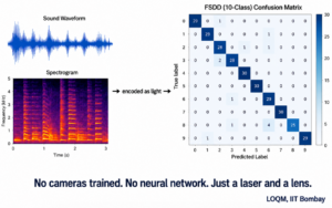 |
Vineetha Joy; Jamshed Palai; Satwik Sahoo; Anshuman Kumar; Amit Sethi; Hema Singh Inverse Design of Metasurface based Absorbers using Physics Guided Conditional Diffusion Models Journal Article In: arXiv preprint, vol. arXiv:2605.19611, 2026. @article{arXiv:2605.19611,
title = {Inverse Design of Metasurface based Absorbers using Physics Guided Conditional Diffusion Models},
author = {Vineetha Joy and Jamshed Palai and Satwik Sahoo and Anshuman Kumar and Amit Sethi and Hema Singh},
url = {https://doi.org/10.48550/arXiv.2605.19611},
doi = {10.48550/arXiv.2605.19611},
year = {2026},
date = {2026-05-19},
journal = {arXiv preprint},
volume = {arXiv:2605.19611},
abstract = {Inverse design of metasurfaces for specific electromagnetic responses requires generating geometries that satisfy stringent spectral constraints while maintaining manufacturability. Conventional design methodologies rely on iterative optimization routines using full wave simulations, which become extremely time consuming and computationally intensive for large design spaces. In addition, commonly employed generative approaches often exhibit limited conditional fidelity and the generated designs often contain fine or irregular features that are impractical to fabricate. In this regard, we propose a physics guided condition quality enhanced diffusion framework for the inverse design of metasurface based absorbers. Here, the conditioning information consisting of target reflection characteristics is integrated into the model using feature wise linear modulation (FiLM). Furthermore, to enforce adherence to target spectra, a pre trained surrogate EM simulator is embedded into the framework introducing physics aware regularization through spectrum level loss functions. The efficiency of the proposed model is demonstrated by generating practically realizable metasurfaces for different types of reflection characteristics in the frequency range of 2 to 18 GHz. The proposed framework achieves an average spectral mean squared error of 0.0006 and band alignment accuracy of 0.958 between the target spectra and the spectra produced by the generated designs, demonstrating high conditional accuracy. In addition, the model generates multiple geometries for the same condition, thereby providing diverse design alternatives to the engineer. The proposed model produces the suitable design in approximately 30 seconds, whereas the conventional approach can take several months under comparable computational resources. The efficiency of the model is also established via experimental measurements.},
keywords = {},
pubstate = {published},
tppubtype = {article}
}
Inverse design of metasurfaces for specific electromagnetic responses requires generating geometries that satisfy stringent spectral constraints while maintaining manufacturability. Conventional design methodologies rely on iterative optimization routines using full wave simulations, which become extremely time consuming and computationally intensive for large design spaces. In addition, commonly employed generative approaches often exhibit limited conditional fidelity and the generated designs often contain fine or irregular features that are impractical to fabricate. In this regard, we propose a physics guided condition quality enhanced diffusion framework for the inverse design of metasurface based absorbers. Here, the conditioning information consisting of target reflection characteristics is integrated into the model using feature wise linear modulation (FiLM). Furthermore, to enforce adherence to target spectra, a pre trained surrogate EM simulator is embedded into the framework introducing physics aware regularization through spectrum level loss functions. The efficiency of the proposed model is demonstrated by generating practically realizable metasurfaces for different types of reflection characteristics in the frequency range of 2 to 18 GHz. The proposed framework achieves an average spectral mean squared error of 0.0006 and band alignment accuracy of 0.958 between the target spectra and the spectra produced by the generated designs, demonstrating high conditional accuracy. In addition, the model generates multiple geometries for the same condition, thereby providing diverse design alternatives to the engineer. The proposed model produces the suitable design in approximately 30 seconds, whereas the conventional approach can take several months under comparable computational resources. The efficiency of the model is also established via experimental measurements. | 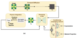 |
Brijesh Kumar; Pavel Tonkaev; Ivan Toftul; Yihong Chen; Vaishakh Unnikrishnan; Albert Mathew; Anshuman Kumar; Furkan Kuruoglu; Filiz Yesilkoy; Yuri Kivshar Intrinsic chirality of dielectric metasurfaces unlocked by resonant chiral modes Journal Article In: arXiv preprint, vol. arXiv:2605.11366 , 2026. @article{https://arxiv.org/abs/2605.11366,
title = {Intrinsic chirality of dielectric metasurfaces unlocked by resonant chiral modes},
author = {Brijesh Kumar and Pavel Tonkaev and Ivan Toftul and Yihong Chen and Vaishakh Unnikrishnan and Albert Mathew and Anshuman Kumar and Furkan Kuruoglu and Filiz Yesilkoy and Yuri Kivshar},
url = {https://doi.org/10.48550/arXiv.2605.11366},
doi = {10.48550/arXiv.2605.11366},
year = {2026},
date = {2026-05-12},
journal = {arXiv preprint},
volume = {arXiv:2605.11366 },
abstract = {Controlling optical chirality at the subwavelength scales is essential for many applications of nanophotonic structures in polarization optics, sensing, and nonlinear photonics. Achieving a strong chiroptical response in planar dielectric metasurfaces without intrinsically chiral building blocks (or "meta-atoms") remains challenging. The recent theoretical study [ACS Photonics 12, 6717 (2025)] predicted that bilayer metasurfaces with rotated C -symmetric apertures can exhibit pronounced chiral response originating from resonant chiral photonic modes realizing maximum chirality under the mode strong coupling. That observation uncovers a novel mechanism of metasurface chirality. Here, we confirm experimentally this novel concept and demonstrate resonantly enhanced circular dichroism in the near-infrared frequency range. We fabricate a free-standing silicon membrane metasurface that is nominally achiral. When out-of-plane symmetry is broken by a thin PMMA layer, it unlocks and activates a strong chiral response. The observed circular dichroism is explained by the properties of chiral photonic modes, and it is governed by interlayer coupling and symmetry breaking, in agreement with theoretical predictions. These results establish bilayer metasurfaces as a simple and versatile platform for engineering strong mode-induced chirality in compact planar photonic metadevices. },
keywords = {},
pubstate = {published},
tppubtype = {article}
}
Controlling optical chirality at the subwavelength scales is essential for many applications of nanophotonic structures in polarization optics, sensing, and nonlinear photonics. Achieving a strong chiroptical response in planar dielectric metasurfaces without intrinsically chiral building blocks (or "meta-atoms") remains challenging. The recent theoretical study [ACS Photonics 12, 6717 (2025)] predicted that bilayer metasurfaces with rotated C -symmetric apertures can exhibit pronounced chiral response originating from resonant chiral photonic modes realizing maximum chirality under the mode strong coupling. That observation uncovers a novel mechanism of metasurface chirality. Here, we confirm experimentally this novel concept and demonstrate resonantly enhanced circular dichroism in the near-infrared frequency range. We fabricate a free-standing silicon membrane metasurface that is nominally achiral. When out-of-plane symmetry is broken by a thin PMMA layer, it unlocks and activates a strong chiral response. The observed circular dichroism is explained by the properties of chiral photonic modes, and it is governed by interlayer coupling and symmetry breaking, in agreement with theoretical predictions. These results establish bilayer metasurfaces as a simple and versatile platform for engineering strong mode-induced chirality in compact planar photonic metadevices. | 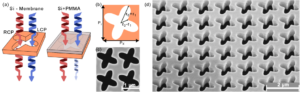 |
Parul Sharma; Sobhan Subhra Mishra; Yash Gupta; Brijesh Kumar; Ranjan Singh; Abhishek Kumar; Anshuman Kumar Active Control of Topological Exceptional Points in Non-Hermitian Metasurfaces Journal Article In: arXiv preprint, vol. arXiv:2605.07702, 2026. @article{ep_active_paper,
title = {Active Control of Topological Exceptional Points in Non-Hermitian Metasurfaces},
author = {Parul Sharma and Sobhan Subhra Mishra and Yash Gupta and Brijesh Kumar and Ranjan Singh and Abhishek Kumar and Anshuman Kumar},
url = {https://doi.org/10.48550/arXiv.2605.07702},
doi = {10.48550/arXiv.2605.07702},
year = {2026},
date = {2026-05-08},
urldate = {2026-05-08},
journal = {arXiv preprint},
volume = {arXiv:2605.07702},
abstract = {Active control and ultrafast switching of non-Hermitian photonic systems are essential for next-generation reconfigurable optical technologies. Here, we demonstrate dynamic temporal manipulation of EPs in the terahertz (THz) regime using optically excited germanium (Ge) as an active medium. By exploiting pump-probe delay as a continuous tuning parameter, we achieve sub-picosecond eigenmode switching (about 0.5 ps) and realize a complete time-resolved EP encirclement within about 2 ps, enabling direct observation of topological phase accumulation. At EP, the metasurface exhibits highly asymmetric transmission for circularly polarized light, characteristic of chiral mode response. Furthermore, we observe ultrafast eigenmode switching and topological phase evolution within about 1 ps, achieving greater than 99 percent cross-polarization modulation depth. The measured results show strong agreement with theoretical modeling, with a high Petermann factor of approximately 10^3, confirming the effectiveness of the design. Our work establishes pump-probe delay time as a dynamical control parameter for EP topology, introducing a new regime of ultrafast non-Hermitian photonics for high-speed switching, enhanced sensitivity, and tunable polarization control in the THz domain.},
keywords = {},
pubstate = {published},
tppubtype = {article}
}
Active control and ultrafast switching of non-Hermitian photonic systems are essential for next-generation reconfigurable optical technologies. Here, we demonstrate dynamic temporal manipulation of EPs in the terahertz (THz) regime using optically excited germanium (Ge) as an active medium. By exploiting pump-probe delay as a continuous tuning parameter, we achieve sub-picosecond eigenmode switching (about 0.5 ps) and realize a complete time-resolved EP encirclement within about 2 ps, enabling direct observation of topological phase accumulation. At EP, the metasurface exhibits highly asymmetric transmission for circularly polarized light, characteristic of chiral mode response. Furthermore, we observe ultrafast eigenmode switching and topological phase evolution within about 1 ps, achieving greater than 99 percent cross-polarization modulation depth. The measured results show strong agreement with theoretical modeling, with a high Petermann factor of approximately 10^3, confirming the effectiveness of the design. Our work establishes pump-probe delay time as a dynamical control parameter for EP topology, introducing a new regime of ultrafast non-Hermitian photonics for high-speed switching, enhanced sensitivity, and tunable polarization control in the THz domain. | 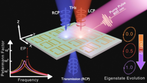 |
Srivatsa Murali; Anshuman Kumar PhoQuPy - A Python framework for Automation of Quantum Optics experiments Journal Article In: arXiv preprint, vol. arXiv:2602.04505, 2026. @article{phoqupyb,
title = {PhoQuPy - A Python framework for Automation of Quantum Optics experiments},
author = {Srivatsa Murali and Anshuman Kumar},
url = {https://doi.org/10.48550/arXiv.2602.04505},
doi = {10.48550/arXiv.2602.04505},
year = {2026},
date = {2026-02-04},
urldate = {2026-02-04},
journal = {arXiv preprint},
volume = {arXiv:2602.04505},
abstract = {We present the automation of a confocal photoluminescence (PL) scanning system for the identification and characterization of single-photon emitters (SPEs) in quantum materials. The setup excites the sample with a laser and acquires a spectrum at each spatial coordinate in a raster scan pattern. A double-acquisition method is used to remove cosmic ray artifacts by comparing subsequent measurements at the same spatial coordinate. Once identified, the emitter is further characterized via a HBT setup, thereby measuring lifetime as well as second-order autocorrelation g(2) measurements to confirm singlephoton emission. The system integrates Python-based hardware control for motorized stages, spectrometer acquisition, and post-processing, with a migration to a galvo-mirror scanning approach for using it along with a cryostat for low temperature measurements. Our results demonstrate spatially resolved PL maps and temperature-dependent spectra, highlighting the capability of the setup to efficiently benchmark SPE performance. We further went on to perform automation of other experiments such as a Non-Linear Interferometry setup for Quantum Imaging with Undetected Light and a Fourier Transform Imaging Spectroscopy using a common path birefringence Interferometer to obtain hyperspectral images of our samples. },
keywords = {},
pubstate = {published},
tppubtype = {article}
}
We present the automation of a confocal photoluminescence (PL) scanning system for the identification and characterization of single-photon emitters (SPEs) in quantum materials. The setup excites the sample with a laser and acquires a spectrum at each spatial coordinate in a raster scan pattern. A double-acquisition method is used to remove cosmic ray artifacts by comparing subsequent measurements at the same spatial coordinate. Once identified, the emitter is further characterized via a HBT setup, thereby measuring lifetime as well as second-order autocorrelation g(2) measurements to confirm singlephoton emission. The system integrates Python-based hardware control for motorized stages, spectrometer acquisition, and post-processing, with a migration to a galvo-mirror scanning approach for using it along with a cryostat for low temperature measurements. Our results demonstrate spatially resolved PL maps and temperature-dependent spectra, highlighting the capability of the setup to efficiently benchmark SPE performance. We further went on to perform automation of other experiments such as a Non-Linear Interferometry setup for Quantum Imaging with Undetected Light and a Fourier Transform Imaging Spectroscopy using a common path birefringence Interferometer to obtain hyperspectral images of our samples. | 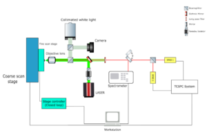 |
Devansh Satra; Abhishek Kumar; Anshuman Kumar Inverse Design of the Topology–Bandwidth Tradeoff in Valley Photonic Crystals Journal Article In: arXiv preprint, vol. arXiv:2601.22958 , 2026. @article{arXiv:2601.22958,
title = {Inverse Design of the Topology–Bandwidth Tradeoff in Valley Photonic Crystals},
author = {Devansh Satra and Abhishek Kumar and Anshuman Kumar},
url = {https://doi.org/10.48550/arXiv.2601.22958},
doi = {10.48550/arXiv.2601.22958},
year = {2026},
date = {2026-01-30},
urldate = {2026-01-30},
journal = {arXiv preprint},
volume = {arXiv:2601.22958 },
abstract = {Integrated on-chip photonics increasingly relies on wave propagation that remains stable in the presence of fabrication imperfections, tight bends, and dense routing. Valley photonic crystals (VPCs) offer an attractive path: by opening a gap at the Dirac points of a hexagonal lattice, one can engineer guided modes confined to domain walls that thread around corners with reduced backreflection. We develop a design framework that co-optimizes the photonic bulk band gap and valley Chern number using a modified particle-swarm optimization (PSO), while evaluating the photonic band structure via plane-wave expansion and the topological characteristics using a gauge-invariant lattice discretization to compute the Berry-curvature. The optimized structures exhibit a clean valley-Hall gap with edge bands traversing the gap and high interface transmission in full-wave simulations. These results consolidate topology-aware geometry optimization for robust on-chip guiding.},
keywords = {},
pubstate = {published},
tppubtype = {article}
}
Integrated on-chip photonics increasingly relies on wave propagation that remains stable in the presence of fabrication imperfections, tight bends, and dense routing. Valley photonic crystals (VPCs) offer an attractive path: by opening a gap at the Dirac points of a hexagonal lattice, one can engineer guided modes confined to domain walls that thread around corners with reduced backreflection. We develop a design framework that co-optimizes the photonic bulk band gap and valley Chern number using a modified particle-swarm optimization (PSO), while evaluating the photonic band structure via plane-wave expansion and the topological characteristics using a gauge-invariant lattice discretization to compute the Berry-curvature. The optimized structures exhibit a clean valley-Hall gap with edge bands traversing the gap and high interface transmission in full-wave simulations. These results consolidate topology-aware geometry optimization for robust on-chip guiding. | 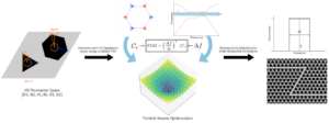 |
Lekshmi Eswaramoorthy; Parul Sharma; Brijesh Kumar; Abhay Anand V S; Anuj Kumar Singh; Kishor Kumar Mandal; Sudha Mokkapati; Anshuman Kumar Focused ion beam polishing based optimization of high-Q silica microdisk resonators Journal Article In: Physica Scripta, vol. 101, no. 4, pp. 045513, 2026. @article{arXiv:2411.06947,
title = {Focused ion beam polishing based optimization of high-Q silica microdisk resonators},
author = {Lekshmi Eswaramoorthy and Parul Sharma and Brijesh Kumar and Abhay Anand V S and Anuj Kumar Singh and Kishor Kumar Mandal and Sudha Mokkapati and Anshuman Kumar},
url = {https://doi.org/10.1088/1402-4896/ae398d},
doi = {https://doi.org/10.1088/1402-4896/ae398d},
year = {2026},
date = {2026-01-29},
urldate = {2026-01-29},
journal = {Physica Scripta},
volume = {101},
number = {4},
pages = {045513},
abstract = {Whispering gallery mode (WGM) microdisk resonators are promising optical devices that confine light efficiently and enable enhanced nonlinear optical effects. This work presents a novel approach to reduce sidewall roughness in SiOtextsubscript{2} microdisk resonators using focused ion beam (FIB) polishing. The microdisks, with varying diameter ranging from 5 to 20 μm are fabricated using a multi-step fabrication scheme. However, the etching process introduces significant sidewall roughness, which increases with decreasing microdisk radius, degrading the resonators' quality. To address this issue, a FIB system is employed to polish the sidewalls, using optimized process parameters to minimize Ga ion implantation. White light interferometry measurements reveal a significant reduction in surface roughness from 7 nm to 20 nm for a 5 μm diameter microdisk, leading to a substantial enhancement in the scattering quality factor (Qss) from 3×10^2 to 2×10^6. These findings demonstrate the effectiveness of FIB polishing in improving the quality of microdisk resonators and open up new possibilities for the fabrication of advanced photonic devices.},
keywords = {},
pubstate = {published},
tppubtype = {article}
}
Whispering gallery mode (WGM) microdisk resonators are promising optical devices that confine light efficiently and enable enhanced nonlinear optical effects. This work presents a novel approach to reduce sidewall roughness in SiOtextsubscript{2} microdisk resonators using focused ion beam (FIB) polishing. The microdisks, with varying diameter ranging from 5 to 20 μm are fabricated using a multi-step fabrication scheme. However, the etching process introduces significant sidewall roughness, which increases with decreasing microdisk radius, degrading the resonators' quality. To address this issue, a FIB system is employed to polish the sidewalls, using optimized process parameters to minimize Ga ion implantation. White light interferometry measurements reveal a significant reduction in surface roughness from 7 nm to 20 nm for a 5 μm diameter microdisk, leading to a substantial enhancement in the scattering quality factor (Qss) from 3×10^2 to 2×10^6. These findings demonstrate the effectiveness of FIB polishing in improving the quality of microdisk resonators and open up new possibilities for the fabrication of advanced photonic devices. |  |
2025
|
Anuj Kumar Singh; Parul Sharma; Kishor Kumar Mandal; Lekshmi Eswaramoorthy; Anshuman Kumar From Atomic Defects to Integrated Photonics: A Perspective on Solid-State Quantum Light Sources Journal Article In: arXiv preprint, vol. arXiv:2512.14402, 2025. @article{arXiv:2512.14402,
title = {From Atomic Defects to Integrated Photonics: A Perspective on Solid-State Quantum Light Sources},
author = {Anuj Kumar Singh and Parul Sharma and Kishor Kumar Mandal and Lekshmi Eswaramoorthy and Anshuman Kumar},
url = {https://doi.org/10.48550/arXiv.2512.14402},
doi = {https://doi.org/10.48550/arXiv.2512.14402},
year = {2025},
date = {2025-12-16},
urldate = {2025-12-16},
journal = {arXiv preprint},
volume = {arXiv:2512.14402},
abstract = {Single-photon emitters (SPEs) constitute a foundational resource for quantum technologies, including secure communication, photonic quantum computing, and emerging quantum network architectures. A wide range of quantum materials, from atom-like point defects in bulk crystals to excitonic states in low-dimensional semiconductors, now provide bright, coherent, and scalable sources of non-classical light. Meanwhile, advances in photonic integration have enabled efficient routing, filtering, and on-chip manipulation of these emitters. From this perspective, we survey and discuss the technological landscape in which solid-state emitters interface with quantum sensing, quantum communication, quantum computation, and emerging photonic AI platforms. Further, we discuss the materials landscape underpinning modern single-photon sources from the zero-dimensional, one-dimensional, two-dimensional and three-dimensional materials. Lastly, we highlight key integration pathways for these single-photon emitters into scalable quantum photonic systems.},
keywords = {},
pubstate = {published},
tppubtype = {article}
}
Single-photon emitters (SPEs) constitute a foundational resource for quantum technologies, including secure communication, photonic quantum computing, and emerging quantum network architectures. A wide range of quantum materials, from atom-like point defects in bulk crystals to excitonic states in low-dimensional semiconductors, now provide bright, coherent, and scalable sources of non-classical light. Meanwhile, advances in photonic integration have enabled efficient routing, filtering, and on-chip manipulation of these emitters. From this perspective, we survey and discuss the technological landscape in which solid-state emitters interface with quantum sensing, quantum communication, quantum computation, and emerging photonic AI platforms. Further, we discuss the materials landscape underpinning modern single-photon sources from the zero-dimensional, one-dimensional, two-dimensional and three-dimensional materials. Lastly, we highlight key integration pathways for these single-photon emitters into scalable quantum photonic systems. | 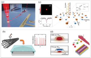 |
Mihir Kumar Sahoo; Abhay Anand V S; Nihar Ranjan Sahoo; Anshuman Kumar Exploring the role of hyperbolicity in surface enhanced Raman sensing Journal Article In: arXiv preprint, vol. arXiv:2511.03387, 2025. @article{arXiv:2511.03387,
title = {Exploring the role of hyperbolicity in surface enhanced Raman sensing},
author = {Mihir Kumar Sahoo and Abhay Anand V S and Nihar Ranjan Sahoo and Anshuman Kumar},
url = {https://doi.org/10.48550/arXiv.2511.03387},
doi = {10.48550/arXiv.2511.03387},
year = {2025},
date = {2025-11-05},
urldate = {2025-11-05},
journal = {arXiv preprint},
volume = {arXiv:2511.03387},
abstract = {A plasmonic nanostructure-based substrate, serving as a surface-enhanced Raman scattering (SERS) substrate, enhances the Raman scattering of molecules. By employing an electron beam lithography followed by our recently developed nano-electroplating protocol, a gold nanorod array SERS substrate can be fabricated to detect lower molecular analyte concentrations, such as Rhodamine 6G (R6G) solution. As the critical dimensions of the nanorod array decrease, they exhibit hyperbolic metamaterial (HMM) characteristics with anisotropic permittivity behavior. In our study, we fabricated two sets of nanorod arrays: one in the HMM regime (140 nm periodicity) and the other in the non-HMM regime (400 nm periodicity), aiming to evaluate the performance of each set based on R6G detection. The obtained results are compared and analyzed using COMSOL simulation and Raman mapping and the role of hyperbolicity is discussed.},
keywords = {},
pubstate = {published},
tppubtype = {article}
}
A plasmonic nanostructure-based substrate, serving as a surface-enhanced Raman scattering (SERS) substrate, enhances the Raman scattering of molecules. By employing an electron beam lithography followed by our recently developed nano-electroplating protocol, a gold nanorod array SERS substrate can be fabricated to detect lower molecular analyte concentrations, such as Rhodamine 6G (R6G) solution. As the critical dimensions of the nanorod array decrease, they exhibit hyperbolic metamaterial (HMM) characteristics with anisotropic permittivity behavior. In our study, we fabricated two sets of nanorod arrays: one in the HMM regime (140 nm periodicity) and the other in the non-HMM regime (400 nm periodicity), aiming to evaluate the performance of each set based on R6G detection. The obtained results are compared and analyzed using COMSOL simulation and Raman mapping and the role of hyperbolicity is discussed. | 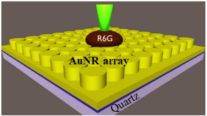 |
Lekshmi Eswaramoorthy; Parul Sharma; Brijesh Kumar; Abhay Anand; Anuj Kumar Singh; Sudha Mokkapati; Anshuman Kumar Protected Ion Beam Fabrication of Two-Dimensional Transition Metal Dichalcogenides based Photonic Devices Journal Article In: arXiv preprint, vol. arXiv:2510.26637 , 2025. @article{arXiv:2510.26637,
title = {Protected Ion Beam Fabrication of Two-Dimensional Transition Metal Dichalcogenides based Photonic Devices},
author = {Lekshmi Eswaramoorthy and Parul Sharma and Brijesh Kumar and Abhay Anand and Anuj Kumar Singh and Sudha Mokkapati and Anshuman Kumar},
url = {https://doi.org/10.48550/arXiv.2510.26637},
doi = {10.48550/arXiv.2510.26637},
year = {2025},
date = {2025-10-30},
urldate = {2025-10-30},
journal = {arXiv preprint},
volume = {arXiv:2510.26637 },
abstract = {Two-dimensional (2D) transition metal dichalcogenides are pivotal for next-generation photonic devices due to their exceptional optical properties and strong light-matter interactions. However, their atomic thinness renders them susceptible to damage during nanoscale fabrication. Focused ion beam technology, while offering precise defect engineering for tailoring optoelectronic properties, often induces collateral damage far beyond the target region, compromising device performance. This study addresses the critical challenge of preserving the intrinsic optical characteristics of 2D TMDCs during FIB patterning. We demonstrate that conventional dielectric encapsulation fails to protect 2D TMDCs from gallium ion-induced damage, leading to persistent defects and quenched optical responses in patterned microstructures. In contrast, polymeric encapsulation with PMMA (polymethyl methacrylate) effectively mitigates damage by acting as a sacrificial layer that absorbs ion impact, thereby preserving the optical properties of the underlying TMDC. Furthermore, we leverage XeF2-assisted Ga ion beam direct patterning, which significantly reduces collateral damage, minimizes Ga ion implantation, and enables precise anisotropic material removal, yielding ultra-smooth sidewalls critical for high-quality photonic resonators. This combined approach of PMMA encapsulation and XeF2-assisted FIB patterning offers a robust, cost-effective, and scalable single-step fabrication route for integrating 2D TMDCs into high-performance photonic devices, thereby maintaining their intrinsic optical functionality essential for advancing quantum technologies and compact optical circuits.},
keywords = {},
pubstate = {published},
tppubtype = {article}
}
Two-dimensional (2D) transition metal dichalcogenides are pivotal for next-generation photonic devices due to their exceptional optical properties and strong light-matter interactions. However, their atomic thinness renders them susceptible to damage during nanoscale fabrication. Focused ion beam technology, while offering precise defect engineering for tailoring optoelectronic properties, often induces collateral damage far beyond the target region, compromising device performance. This study addresses the critical challenge of preserving the intrinsic optical characteristics of 2D TMDCs during FIB patterning. We demonstrate that conventional dielectric encapsulation fails to protect 2D TMDCs from gallium ion-induced damage, leading to persistent defects and quenched optical responses in patterned microstructures. In contrast, polymeric encapsulation with PMMA (polymethyl methacrylate) effectively mitigates damage by acting as a sacrificial layer that absorbs ion impact, thereby preserving the optical properties of the underlying TMDC. Furthermore, we leverage XeF2-assisted Ga ion beam direct patterning, which significantly reduces collateral damage, minimizes Ga ion implantation, and enables precise anisotropic material removal, yielding ultra-smooth sidewalls critical for high-quality photonic resonators. This combined approach of PMMA encapsulation and XeF2-assisted FIB patterning offers a robust, cost-effective, and scalable single-step fabrication route for integrating 2D TMDCs into high-performance photonic devices, thereby maintaining their intrinsic optical functionality essential for advancing quantum technologies and compact optical circuits. | 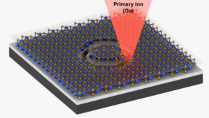 |
Poulomi Chakrabarty; Sera Sen; Anwesha Chakraborty; Abhay Anand VS; Srilagna Sahoo; Anshuman Kumar; Debjani Karmakar; Saurabh Lodha Electrostatically Controlled Pyrophototronic Effect in Strain‐Polarized WS2 for an Accident Alert System Journal Article In: Advanced Functional Materials, vol. 36, no. 15, pp. e17870, 2025. @article{10.1002/adfm.202517870,
title = {Electrostatically Controlled Pyrophototronic Effect in Strain‐Polarized WS2 for an Accident Alert System},
author = {Poulomi Chakrabarty and Sera Sen and Anwesha Chakraborty and Abhay Anand VS and Srilagna Sahoo and Anshuman Kumar and Debjani Karmakar and Saurabh Lodha},
url = {https://doi.org/10.1002/adfm.202517870},
doi = {10.1002/adfm.202517870},
year = {2025},
date = {2025-09-25},
urldate = {2025-09-25},
journal = {Advanced Functional Materials},
volume = {36},
number = {15},
pages = {e17870},
abstract = {Event-based dynamic light detection, specifically in low illumination environments, is a critical requirement in autonomous vehicles. This work reports low optical power photodetection through the dynamic pyrophototronic effect in an ultra-thin 2D WS2 phototransistor. A four-stage pyrophototronic photoresponse has been realized through biaxial strain-polarization of the non-centrosymmetric (5-layer) WS2 channel using a sub-wavelength, nanopatterned hBN gate dielectric. Presence of strain in WS2 has been verified through extensive spectroscopic characterization, and that of strain-induced charge polarization through density functional theory calculations, as well as piezo force microscopy. The pyrophototronic effect boosts dynamic photoresponsivity (0.7 A W−1) and detectivity (1.2 × 10¹⁵ Jones cm−1) by up to 8x, and enhances the photodetection speed by 3x over the non-patterned (unstrained) phototransistor, demonstrating a path to ameliorating the responsivity-speed trade-off in 2D photodetectors. Analysis of gate voltage, wavelength, and optical power dependence of the pyrophototronic current through measurements and band physics highlights its prominence under low channel population of electrostatically- or optically-induced free carriers. Gate tunability of the pyrophototronic current is leveraged to design an optical spike-triggered dynamic accident alert system with speed-specific control for self-driving applications under low light conditions.},
keywords = {},
pubstate = {published},
tppubtype = {article}
}
Event-based dynamic light detection, specifically in low illumination environments, is a critical requirement in autonomous vehicles. This work reports low optical power photodetection through the dynamic pyrophototronic effect in an ultra-thin 2D WS2 phototransistor. A four-stage pyrophototronic photoresponse has been realized through biaxial strain-polarization of the non-centrosymmetric (5-layer) WS2 channel using a sub-wavelength, nanopatterned hBN gate dielectric. Presence of strain in WS2 has been verified through extensive spectroscopic characterization, and that of strain-induced charge polarization through density functional theory calculations, as well as piezo force microscopy. The pyrophototronic effect boosts dynamic photoresponsivity (0.7 A W−1) and detectivity (1.2 × 10¹⁵ Jones cm−1) by up to 8x, and enhances the photodetection speed by 3x over the non-patterned (unstrained) phototransistor, demonstrating a path to ameliorating the responsivity-speed trade-off in 2D photodetectors. Analysis of gate voltage, wavelength, and optical power dependence of the pyrophototronic current through measurements and band physics highlights its prominence under low channel population of electrostatically- or optically-induced free carriers. Gate tunability of the pyrophototronic current is leveraged to design an optical spike-triggered dynamic accident alert system with speed-specific control for self-driving applications under low light conditions. | 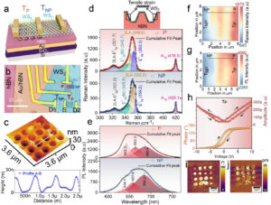 |
Brijesh Kumar; Elizaveta Tsiplakova; Samuel John; Parul Sharma; Nikolay Solodovchenko; Andrey Bogdanov; Shriganesh S. Prabhu; Abhishek Kumar; Anshuman Kumar Sensing with Broken Symmetry: Revisiting Bound States in the Continuum Journal Article In: arXiv preprint, vol. arXiv:2507.05676, 2025. @article{arXiv:2507.05676,
title = {Sensing with Broken Symmetry: Revisiting Bound States in the Continuum},
author = {Brijesh Kumar and Elizaveta Tsiplakova and Samuel John and Parul Sharma and Nikolay Solodovchenko and Andrey Bogdanov and Shriganesh S. Prabhu and Abhishek Kumar and Anshuman Kumar},
url = {https://doi.org/10.48550/arXiv.2507.05676},
doi = {10.48550/arXiv.2507.05676},
year = {2025},
date = {2025-07-08},
urldate = {2025-07-08},
journal = {arXiv preprint},
volume = {arXiv:2507.05676},
abstract = {Metasurface with bound states in the continuum (BICs) offer exceptional potential for optical sensing due to their inherently high quality (Q) factors. However, the detection of symmetry-protected BICs remains experimentally challenging due to their non-radiative nature. Introducing slight asymmetry makes these resonances observable, though it reduces the Q-factor. In real devices, intrinsic material losses further affect the resonance behavior and sensing performance. While it is often assumed that sensing is optimized at the critical coupling when radiative and non-radiative losses are balanced, the precise conditions for achieving the best limit of detection (LOD) and figure-of-merit (FOM) remain under active discussion. In this work, we experimentally and theoretically investigate BIC-based sensing in the terahertz (THz) range. We demonstrate that the LOD exhibits a non-monotonic dependence on asymmetry, reaching an unexpected optimum where radiative and non-radiative losses are not equal. Moreover, we show that this optimum differs between reflection and transmission sensing schemes. Our results provide practical guidelines for optimizing Q-factor, sensitivity, and signal amplitude together, and contribute to a deeper understanding of the fundamental limits of BIC-based sensing.},
keywords = {},
pubstate = {published},
tppubtype = {article}
}
Metasurface with bound states in the continuum (BICs) offer exceptional potential for optical sensing due to their inherently high quality (Q) factors. However, the detection of symmetry-protected BICs remains experimentally challenging due to their non-radiative nature. Introducing slight asymmetry makes these resonances observable, though it reduces the Q-factor. In real devices, intrinsic material losses further affect the resonance behavior and sensing performance. While it is often assumed that sensing is optimized at the critical coupling when radiative and non-radiative losses are balanced, the precise conditions for achieving the best limit of detection (LOD) and figure-of-merit (FOM) remain under active discussion. In this work, we experimentally and theoretically investigate BIC-based sensing in the terahertz (THz) range. We demonstrate that the LOD exhibits a non-monotonic dependence on asymmetry, reaching an unexpected optimum where radiative and non-radiative losses are not equal. Moreover, we show that this optimum differs between reflection and transmission sensing schemes. Our results provide practical guidelines for optimizing Q-factor, sensitivity, and signal amplitude together, and contribute to a deeper understanding of the fundamental limits of BIC-based sensing. | 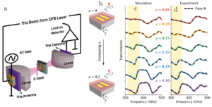 |
Anuj Kumar Singh; Utkarsh Utkarsh; Pablo Tieben; Kishor Kumar Mandal; Brijesh Kumar; Rishabh Vij; Amrita Majumder; Ikshvaku Shyam; Shagun Kumar; Kenji Watanabe; Takashi Taniguchi; Venu Gopal Achanta; Andreas W Schell; Anshuman Kumar Plasmonic‐Strain Engineering of Quantum Emitters in Hexagonal Boron Nitride Journal Article In: Advanced Materials Interfaces, pp. 2500071, 2025. @article{arXiv:2401.11428,
title = {Plasmonic‐Strain Engineering of Quantum Emitters in Hexagonal Boron Nitride},
author = {Anuj Kumar Singh and Utkarsh Utkarsh and Pablo Tieben and Kishor Kumar Mandal and Brijesh Kumar and Rishabh Vij and Amrita Majumder and Ikshvaku Shyam and Shagun Kumar and Kenji Watanabe and Takashi Taniguchi and Venu Gopal Achanta and Andreas W Schell and Anshuman Kumar},
url = {https://doi.org/10.1002/admi.202500071},
doi = {10.1002/admi.202500071},
year = {2025},
date = {2025-06-05},
urldate = {2025-06-05},
journal = {Advanced Materials Interfaces},
pages = {2500071},
abstract = {In the realm of quantum information and sensing, there has been substantial interest in the single-photon emission (SPE) associated with defects in hexagonal boron nitride (hBN). With the goal of producing deterministic emission centers, in this work, a platform is presented for engineering emission in hBN integrated with gold (Au) truncated nanocone structures. These findings highlight that, the emission in the hBN overlaps with the emission due to the truncated gold nanocones. Furthermore, the quantum characteristics of this emission are measured and found that while this system demonstrates support for SPE, the origin of this emission remains ambiguous. Specifically, it is unclear whether the emission arises from defects generated by the induced strain or from alternative defect mechanisms. This uncertainty stems from the fluorescence properties inherent to gold, complicating the definitive attribution of the quantum emission source. To provide a rigorous theoretical foundation, the effects of strain are elucidated via the Kirchhoff–Love theory. Additionally, the enhancements observed due to plasmonic effects are comprehensively explained through the resolution of Maxwell's equations. This study will be useful for the development of deterministic and tunable single photonic sources in 2D materials and their integration with plasmonic platforms.},
keywords = {},
pubstate = {published},
tppubtype = {article}
}
In the realm of quantum information and sensing, there has been substantial interest in the single-photon emission (SPE) associated with defects in hexagonal boron nitride (hBN). With the goal of producing deterministic emission centers, in this work, a platform is presented for engineering emission in hBN integrated with gold (Au) truncated nanocone structures. These findings highlight that, the emission in the hBN overlaps with the emission due to the truncated gold nanocones. Furthermore, the quantum characteristics of this emission are measured and found that while this system demonstrates support for SPE, the origin of this emission remains ambiguous. Specifically, it is unclear whether the emission arises from defects generated by the induced strain or from alternative defect mechanisms. This uncertainty stems from the fluorescence properties inherent to gold, complicating the definitive attribution of the quantum emission source. To provide a rigorous theoretical foundation, the effects of strain are elucidated via the Kirchhoff–Love theory. Additionally, the enhancements observed due to plasmonic effects are comprehensively explained through the resolution of Maxwell's equations. This study will be useful for the development of deterministic and tunable single photonic sources in 2D materials and their integration with plasmonic platforms. |  |
Vineetha Joy; Aditya Anand; Nidhi; Anshuman Kumar; Amit Sethi; Hema Singh A Surrogate Model for the Forward Design of Multi-layered Metasurface-based Radar Absorbing Structures Journal Article In: arXiv preprint, vol. arXiv:2505.09251, 2025. @article{arXiv:2505.09251,
title = {A Surrogate Model for the Forward Design of Multi-layered Metasurface-based Radar Absorbing Structures},
author = {Vineetha Joy and Aditya Anand and Nidhi and Anshuman Kumar and Amit Sethi and Hema Singh},
url = {https://doi.org/10.48550/arXiv.2505.09251},
doi = {10.48550/arXiv.2505.09251},
year = {2025},
date = {2025-05-14},
journal = {arXiv preprint},
volume = {arXiv:2505.09251},
abstract = {Metasurface-based radar absorbing structures (RAS) are highly preferred for applications like stealth technology, electromagnetic (EM) shielding, etc. due to their capability to achieve frequency selective absorption characteristics with minimal thickness and reduced weight penalty. However, the conventional approach for the EM design and optimization of these structures relies on forward simulations, using full wave simulation tools, to predict the electromagnetic (EM) response of candidate meta atoms. This process is computationally intensive, extremely time consuming and requires exploration of large design spaces. To overcome this challenge, we propose a surrogate model that significantly accelerates the prediction of EM responses of multi-layered metasurface-based RAS. A convolutional neural network (CNN) based architecture with Huber loss function has been employed to estimate the reflection characteristics of the RAS model. The proposed model achieved a cosine similarity of 99.9 percent and a mean square error of 0.001 within 1000 epochs of training. The efficiency of the model has been established via full wave simulations as well as experiment where it demonstrated significant reduction in computational time while maintaining high predictive accuracy.},
keywords = {},
pubstate = {published},
tppubtype = {article}
}
Metasurface-based radar absorbing structures (RAS) are highly preferred for applications like stealth technology, electromagnetic (EM) shielding, etc. due to their capability to achieve frequency selective absorption characteristics with minimal thickness and reduced weight penalty. However, the conventional approach for the EM design and optimization of these structures relies on forward simulations, using full wave simulation tools, to predict the electromagnetic (EM) response of candidate meta atoms. This process is computationally intensive, extremely time consuming and requires exploration of large design spaces. To overcome this challenge, we propose a surrogate model that significantly accelerates the prediction of EM responses of multi-layered metasurface-based RAS. A convolutional neural network (CNN) based architecture with Huber loss function has been employed to estimate the reflection characteristics of the RAS model. The proposed model achieved a cosine similarity of 99.9 percent and a mean square error of 0.001 within 1000 epochs of training. The efficiency of the model has been established via full wave simulations as well as experiment where it demonstrated significant reduction in computational time while maintaining high predictive accuracy. | 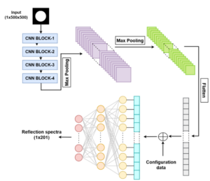 |
2024
|
Reyhan Mehta; Anshuman Kumar Quantum emitters in bilayer hexagonal boron nitride Journal Article In: arXiv preprint, vol. arXiv:2411.09346, 2024. @article{arXiv:2411.09346,
title = {Quantum emitters in bilayer hexagonal boron nitride},
author = {Reyhan Mehta and Anshuman Kumar},
url = {https://doi.org/10.48550/arXiv.2411.09346},
doi = {10.48550/arXiv.2411.09346},
year = {2024},
date = {2024-11-15},
urldate = {2024-11-15},
journal = {arXiv preprint},
volume = {arXiv:2411.09346},
abstract = {Hexagonal boron nitride (hBN) has been experimentally shown to exhibit room-temperature single-photon emission. This emission is attributed to defect states in the wide band-gap of hBN, which allow new optical transitions between these dispersion-less defect levels. In this work, we study the new spectral features introduced by interacting atomic defects in consecutive layers of bilayer hBN. Density Functional theory simulations have been carried out to calculate the energy band structure, frequency-dependent complex dielectric functions, and Kohn-Sham states to demonstrate and understand the cause of the emission enhancements. We found that placing colour centres in the vicinity of each other in bilayer hBN introduces new polarization dependent spectral features, with strong dependence on the distance and relative orientation between atomic defects. Our results provide a pathway to engineering single photon emission in hBN via inter-defect interaction.},
keywords = {},
pubstate = {published},
tppubtype = {article}
}
Hexagonal boron nitride (hBN) has been experimentally shown to exhibit room-temperature single-photon emission. This emission is attributed to defect states in the wide band-gap of hBN, which allow new optical transitions between these dispersion-less defect levels. In this work, we study the new spectral features introduced by interacting atomic defects in consecutive layers of bilayer hBN. Density Functional theory simulations have been carried out to calculate the energy band structure, frequency-dependent complex dielectric functions, and Kohn-Sham states to demonstrate and understand the cause of the emission enhancements. We found that placing colour centres in the vicinity of each other in bilayer hBN introduces new polarization dependent spectral features, with strong dependence on the distance and relative orientation between atomic defects. Our results provide a pathway to engineering single photon emission in hBN via inter-defect interaction. |  |
Nihar Ranjan Sahoo; S S Jatin Prasath; Brijesh Kumar; Anshuman Kumar Twisted hyperbolic van der Waals crystals for chip-scale full Stokes mid-infrared polarization detection Journal Article In: Journal of Physics D: Applied Physics, vol. 57, no. 50, pp. 505104, 2024. @article{stokes_polarimeter,
title = {Twisted hyperbolic van der Waals crystals for chip-scale full Stokes mid-infrared polarization detection},
author = {Nihar Ranjan Sahoo and S S Jatin Prasath and Brijesh Kumar and Anshuman Kumar},
url = {https://iopscience.iop.org/article/10.1088/1361-6463/ad7a85},
doi = {10.1088/1361-6463/ad7a85},
year = {2024},
date = {2024-09-25},
urldate = {2024-09-25},
journal = {Journal of Physics D: Applied Physics},
volume = {57},
number = {50},
pages = {505104},
abstract = {Investigating the polarization properties of light in the mid-infrared (mid-IR) spectrum is crucial for molecular sensing, biomedical diagnostics, and IR imaging system technologies. Traditional methods, limited by bulky size and complicated fabrication process, utilize large rotating optics for full Stokes polarization detection, impeding miniaturization and accuracy. Naturally occurring hyperbolic van der Waals (vdW) material based devices can address these challenges due to their lithography-free fabrication, ease of integration with chip-scale platforms and room-temperature operation. This study designs a chip-integrated polarimeter by performing multi-objective optimization for efficient exploration of the design parameter space. The spatial division measurement scheme used incorporates six precisely designed linear and circular polarization filters, achieving high extinction ratios exceeding 30 dB and transmittance surpassing 50
keywords = {},
pubstate = {published},
tppubtype = {article}
}
Investigating the polarization properties of light in the mid-infrared (mid-IR) spectrum is crucial for molecular sensing, biomedical diagnostics, and IR imaging system technologies. Traditional methods, limited by bulky size and complicated fabrication process, utilize large rotating optics for full Stokes polarization detection, impeding miniaturization and accuracy. Naturally occurring hyperbolic van der Waals (vdW) material based devices can address these challenges due to their lithography-free fabrication, ease of integration with chip-scale platforms and room-temperature operation. This study designs a chip-integrated polarimeter by performing multi-objective optimization for efficient exploration of the design parameter space. The spatial division measurement scheme used incorporates six precisely designed linear and circular polarization filters, achieving high extinction ratios exceeding 30 dB and transmittance surpassing 50
title = { Exceptional point sensing via energy loss profile in a non-Hermitian system},
author = {Parul Sharma and Brijesh Kumar and Nihar Ranjan Sahoo and Anshuman Kumar},
url = {https://doi.org/10.1016/j.sna.2024.115681},
doi = {10.1016/j.sna.2024.115681},
year = {2024},
date = {2024-08-16},
urldate = {2024-08-16},
journal = {Sensors and Actuators A: Physical},
volume = {378},
pages = {115681},
abstract = {The heightened sensitivity observed in non-Hermitian systems at exceptional points (EPs) has garnered significant attention. Typical EP sensor implementations rely on precise measurements of spectra and importantly, for real time sensing measurements, the EP condition ceases to hold as the perturbation increases over time, thereby preventing the use of high sensitivity at the EP point. In this work, we present an new approach to EP sensing which goes beyond these two traditional constraints. Firstly, instead of measuring the spectra, our scheme of EP based sensing is based on the observation of decay length of the optical mode in finite size gratings, which is validated via coupled mode theory as well as full wave electrodynamic simulations. Secondly, for larger perturbation strengths, the EP is spectrally shifted instead of being destroyed — this spectral shift of the EP is calibrated and using this look-up table, we propose continuous real time detection by varying the excitation laser wavelength. As a proof of principle of our technique, we present an application to the sensing of coronavirus particles, which shows unprecedented limit of detection. Furthermore, our analysis includes calculation of the signal-to-noise ratio, revealing that EP sensors offer advantage when classical technical noise dominates over fundamental noise. These findings will contribute to the expanding field of exceptional point based sensing technologies for real time applications beyond spectral measurements.},
keywords = {},
pubstate = {published},
tppubtype = {article}
}
The heightened sensitivity observed in non-Hermitian systems at exceptional points (EPs) has garnered significant attention. Typical EP sensor implementations rely on precise measurements of spectra and importantly, for real time sensing measurements, the EP condition ceases to hold as the perturbation increases over time, thereby preventing the use of high sensitivity at the EP point. In this work, we present an new approach to EP sensing which goes beyond these two traditional constraints. Firstly, instead of measuring the spectra, our scheme of EP based sensing is based on the observation of decay length of the optical mode in finite size gratings, which is validated via coupled mode theory as well as full wave electrodynamic simulations. Secondly, for larger perturbation strengths, the EP is spectrally shifted instead of being destroyed — this spectral shift of the EP is calibrated and using this look-up table, we propose continuous real time detection by varying the excitation laser wavelength. As a proof of principle of our technique, we present an application to the sensing of coronavirus particles, which shows unprecedented limit of detection. Furthermore, our analysis includes calculation of the signal-to-noise ratio, revealing that EP sensors offer advantage when classical technical noise dominates over fundamental noise. These findings will contribute to the expanding field of exceptional point based sensing technologies for real time applications beyond spectral measurements. | 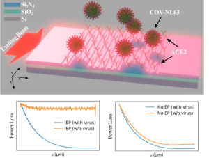 |
Nihar Ranjan Sahoo; Brijesh Kumar; S.S. Jatin Prasath; Saurabh Dixit; Rohit Kumar; Aneesh Bapat; Parul Sharma; Joshua Caldwell; Anshuman Kumar Polaritons in photonic hypercrystals of van der Waals materials Journal Article In: Advanced Functional Materials, pp. 2316863, 2024. @article{arXiv:2309.17146,
title = {Polaritons in photonic hypercrystals of van der Waals materials},
author = {Nihar Ranjan Sahoo and Brijesh Kumar and S.S. Jatin Prasath and Saurabh Dixit and Rohit Kumar and Aneesh Bapat and Parul Sharma and Joshua Caldwell and Anshuman Kumar},
url = {https://doi.org/10.1002/adfm.202316863},
doi = {10.1002/adfm.202316863},
year = {2024},
date = {2024-07-26},
urldate = {2024-07-26},
journal = {Advanced Functional Materials},
pages = {2316863},
abstract = {In-plane Hyperbolic Phonon polaritons (HPhPs) are quasiparticles formed via coupling of photons and optical phonons in in-plane hyperbolic materials and offer unique applications in sensing, thermal emitters and high resolution imaging. However, the large momentum mismatch between photons and these in-plane HPhPs has restricted their technological potential as most experimental demonstration rely on sophisticated and expensive near field detection schemes. In this work, using the example of α−MoO3, we demonstrate that by constructing photonic hypercrystals of this material, one can not only excite these in-plane HPhPs in the far field but also tune the far field response via twisting the hypercrystal lattice with respect the lattice of α−MoO3. Our findings will pave the way for the development of practical in-plane HPhP devices as well as provide access to new fundamental physics of such materials via conventional and well developed far field measurement techniques.},
keywords = {},
pubstate = {published},
tppubtype = {article}
}
In-plane Hyperbolic Phonon polaritons (HPhPs) are quasiparticles formed via coupling of photons and optical phonons in in-plane hyperbolic materials and offer unique applications in sensing, thermal emitters and high resolution imaging. However, the large momentum mismatch between photons and these in-plane HPhPs has restricted their technological potential as most experimental demonstration rely on sophisticated and expensive near field detection schemes. In this work, using the example of α−MoO3, we demonstrate that by constructing photonic hypercrystals of this material, one can not only excite these in-plane HPhPs in the far field but also tune the far field response via twisting the hypercrystal lattice with respect the lattice of α−MoO3. Our findings will pave the way for the development of practical in-plane HPhP devices as well as provide access to new fundamental physics of such materials via conventional and well developed far field measurement techniques. |  |
Mahesh Bhupati; Abhishek Mall; Anshuman Kumar; Pankaj K Jha Deep learning-based variational autoencoder for classification of quantum and classical states of light Journal Article In: arXiv preprint, vol. arXiv:2405.05243, 2024. @article{arXiv:2405.05243,
title = {Deep learning-based variational autoencoder for classification of quantum and classical states of light},
author = {Mahesh Bhupati and Abhishek Mall and Anshuman Kumar and Pankaj K Jha},
url = {https://doi.org/10.48550/arXiv.2405.05243},
doi = {10.48550/arXiv.2405.05243},
year = {2024},
date = {2024-05-08},
urldate = {2024-05-08},
journal = {arXiv preprint},
volume = {arXiv:2405.05243},
abstract = {Advancements in optical quantum technologies have been enabled by the generation, manipulation, and characterization of light, with identification based on its photon statistics. However, characterizing light and its sources through single photon measurements often requires efficient detectors and longer measurement times to obtain high-quality photon statistics. Here we introduce a deep learning-based variational autoencoder (VAE) method for classifying single photon added coherent state (SPACS), single photon added thermal state (SPACS), mixed states between coherent/SPACS and thermal/SPATS of light. Our semisupervised learning-based VAE efficiently maps the photon statistics features of light to a lower dimension, enabling quasi-instantaneous classification with low average photon counts. The proposed VAE method is robust and maintains classification accuracy in the presence of losses inherent in an experiment, such as finite collection efficiency, non-unity quantum efficiency, finite number of detectors, etc. Additionally, leveraging the transfer learning capabilities of VAE enables successful classification of data of any quality using a single trained model. We envision that such a deep learning methodology will enable better classification of quantum light and light sources even in the presence of poor detection quality.},
keywords = {},
pubstate = {published},
tppubtype = {article}
}
Advancements in optical quantum technologies have been enabled by the generation, manipulation, and characterization of light, with identification based on its photon statistics. However, characterizing light and its sources through single photon measurements often requires efficient detectors and longer measurement times to obtain high-quality photon statistics. Here we introduce a deep learning-based variational autoencoder (VAE) method for classifying single photon added coherent state (SPACS), single photon added thermal state (SPACS), mixed states between coherent/SPACS and thermal/SPATS of light. Our semisupervised learning-based VAE efficiently maps the photon statistics features of light to a lower dimension, enabling quasi-instantaneous classification with low average photon counts. The proposed VAE method is robust and maintains classification accuracy in the presence of losses inherent in an experiment, such as finite collection efficiency, non-unity quantum efficiency, finite number of detectors, etc. Additionally, leveraging the transfer learning capabilities of VAE enables successful classification of data of any quality using a single trained model. We envision that such a deep learning methodology will enable better classification of quantum light and light sources even in the presence of poor detection quality. |  |
Kishor Kumar Mandal; Anuj Kumar Singh; Brijesh Kumar; Amit P Shah; Rishabh Vij; Amrita Majumder; Janhavi Jayawant Khunte; Venu Gopal Achanta; Anshuman Kumar Emission engineering in monolithically integrated silicon nitride microring resonators Journal Article In: ACS Materials Letters, vol. 6, pp. 1831–1840, 2024. @article{arXiv:2401.04963,
title = {Emission engineering in monolithically integrated silicon nitride microring resonators},
author = {Kishor Kumar Mandal and Anuj Kumar Singh and Brijesh Kumar and Amit P Shah and Rishabh Vij and Amrita Majumder and Janhavi Jayawant Khunte and Venu Gopal Achanta and Anshuman Kumar},
url = {https://doi.org/10.1021/acsmaterialslett.4c00105},
doi = {10.1021/acsmaterialslett.4c00105},
year = {2024},
date = {2024-04-05},
urldate = {2024-04-05},
journal = {ACS Materials Letters},
volume = {6},
pages = {1831--1840},
abstract = {Monolithic integration of solid-state color centers with photonic elements of the same material is a promising approach to overcome the constraints of fabrication complexity and coupling losses in traditional hybrid integration approaches. A wide band-gap, low-loss silicon nitride (SiN) platform is a mature technology, having CMOS compatibility, widely used in hybrid integrated photonics and optoelectronics. However, it has been shown that certain growth conditions enable the SiN material to host color centers, whose origin is currently under investigation. In this work, we have engineered a novel technique for the efficient coupling of these intrinsic emitters into the whispering gallery modes (WGMs) of the SiN microring cavity -- which has not been explored previously. We have engineered a subwavelength-sized notch into the rim of the SiN microring structure, to optimize the collection efficiency of the cavity-coupled enhanced photoluminescence (PL) spectra at room temperature. The platform presented in this work will enable the development of monolithic integration of color centers with nanophotonic elements for application to quantum photonic technologies.},
keywords = {},
pubstate = {published},
tppubtype = {article}
}
Monolithic integration of solid-state color centers with photonic elements of the same material is a promising approach to overcome the constraints of fabrication complexity and coupling losses in traditional hybrid integration approaches. A wide band-gap, low-loss silicon nitride (SiN) platform is a mature technology, having CMOS compatibility, widely used in hybrid integrated photonics and optoelectronics. However, it has been shown that certain growth conditions enable the SiN material to host color centers, whose origin is currently under investigation. In this work, we have engineered a novel technique for the efficient coupling of these intrinsic emitters into the whispering gallery modes (WGMs) of the SiN microring cavity -- which has not been explored previously. We have engineered a subwavelength-sized notch into the rim of the SiN microring structure, to optimize the collection efficiency of the cavity-coupled enhanced photoluminescence (PL) spectra at room temperature. The platform presented in this work will enable the development of monolithic integration of color centers with nanophotonic elements for application to quantum photonic technologies. |  |
Hongwei Wang*; Anshuman Kumar*; Siyuan Dai; Xiao Lin; Zubin Jacob; Sang-Hyun Oh; Vinod Menon; Evgenii Narimanov; Young Duck Kim; Jian-Ping Wang; Phaedon Avouris; Luis Martin Moreno; Joshua Caldwell; Tony Low Planar hyperbolic polaritons in 2D van der Waals materials Journal Article In: Nature Comunications, vol. 15, no. 69, 2024. @article{natcom2023_1,
title = {Planar hyperbolic polaritons in 2D van der Waals materials},
author = {Hongwei Wang* and Anshuman Kumar* and Siyuan Dai and Xiao Lin and Zubin Jacob and Sang-Hyun Oh and Vinod Menon and Evgenii Narimanov and Young Duck Kim and Jian-Ping Wang and Phaedon Avouris and Luis Martin Moreno and Joshua Caldwell and Tony Low },
url = {https://doi.org/10.1038/s41467-023-43992-8},
doi = {10.1038/s41467-023-43992-8},
year = {2024},
date = {2024-01-02},
urldate = {2024-01-02},
journal = {Nature Comunications},
volume = {15},
number = {69},
abstract = {Anisotropic planar polaritons - hybrid electromagnetic modes mediated by phonons, plasmons, or excitons - in biaxial two-dimensional (2D) van der Waals crystals have attracted significant attention due to their fundamental physics and potential nanophotonic applications. In this Perspective, we review the properties of planar hyperbolic polaritons and the variety of methods that can be used to experimentally tune them. We argue that such natural, planar hyperbolic media should be fairly common in biaxial and uniaxial 2D and 1D van der Waals crystals, and identify the untapped opportunities they could enable for functional (i.e. ferromagnetic, ferroelectric, and piezoelectric) polaritons. Lastly, we provide our perspectives on the technological applications of such planar hyperbolic polaritons.},
keywords = {},
pubstate = {published},
tppubtype = {article}
}
Anisotropic planar polaritons - hybrid electromagnetic modes mediated by phonons, plasmons, or excitons - in biaxial two-dimensional (2D) van der Waals crystals have attracted significant attention due to their fundamental physics and potential nanophotonic applications. In this Perspective, we review the properties of planar hyperbolic polaritons and the variety of methods that can be used to experimentally tune them. We argue that such natural, planar hyperbolic media should be fairly common in biaxial and uniaxial 2D and 1D van der Waals crystals, and identify the untapped opportunities they could enable for functional (i.e. ferromagnetic, ferroelectric, and piezoelectric) polaritons. Lastly, we provide our perspectives on the technological applications of such planar hyperbolic polaritons. | 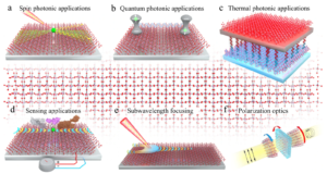 |
2023
|
Abhay Anand V S; Mihir Kumar Sahoo; Faiha Mujeeb; Abin Varghese; Subhabrata Dhar; Saurabh Lodha; Anshuman Kumar Novel Nano-Electroplating-Based Plasmonic Platform for Giant Emission Enhancement in Monolayer Semiconductors Journal Article In: ACS Applied Materials & Interfaces, vol. 15, no. 49, pp. 57783-57790, 2023. @article{arXiv:2306.13507,
title = {Novel Nano-Electroplating-Based Plasmonic Platform for Giant Emission Enhancement in Monolayer Semiconductors},
author = {Abhay Anand V S and Mihir Kumar Sahoo and Faiha Mujeeb and Abin Varghese and Subhabrata Dhar and Saurabh Lodha and Anshuman Kumar},
url = {https://doi.org/10.1021/acsami.3c11564},
doi = {10.1021/acsami.3c11564},
year = {2023},
date = {2023-12-04},
urldate = {2023-12-04},
journal = {ACS Applied Materials & Interfaces},
volume = {15},
number = {49},
pages = {57783-57790},
abstract = {Two dimensional semiconductors have attracted considerable attention owing to their exceptional electronic and optical characteristics. However, their practical application has been hindered by the limited light absorption resulting from their atomically thin thickness and low quantum yield. A highly effective approach to manipulate optical properties and address these limitations is integrating subwavelength plasmonic nanostructures with these monolayers. In this study, we employed electron beam lithography and electroplating technique to fabricate a gold nanodisc (AuND) array capable of enhancing the photoluminescence (PL) of monolayer MoS2 giantly. Monolayer MoS2 placed on the top of the AuND array yields up to 150-fold PL enhancement compared to that on a gold film. We explain our experimental findings based on electromagnetic simulations.},
keywords = {},
pubstate = {published},
tppubtype = {article}
}
Two dimensional semiconductors have attracted considerable attention owing to their exceptional electronic and optical characteristics. However, their practical application has been hindered by the limited light absorption resulting from their atomically thin thickness and low quantum yield. A highly effective approach to manipulate optical properties and address these limitations is integrating subwavelength plasmonic nanostructures with these monolayers. In this study, we employed electron beam lithography and electroplating technique to fabricate a gold nanodisc (AuND) array capable of enhancing the photoluminescence (PL) of monolayer MoS2 giantly. Monolayer MoS2 placed on the top of the AuND array yields up to 150-fold PL enhancement compared to that on a gold film. We explain our experimental findings based on electromagnetic simulations. | 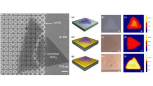 |
Brijesh Kumar; Anuj Kumar Singh; Kishor K Mandal; Parul Sharma; Nihar Ranjan Sahoo; Anshuman Kumar A universal and stable metasurface for photonic quasi bound state in continuum coupled with two dimensional semiconductors Journal Article In: Journal of Physics D: Applied Physics, vol. 56, no. 42, pp. 425105, 2023. @article{arXiv:2212.05951,
title = {A universal and stable metasurface for photonic quasi bound state in continuum coupled with two dimensional semiconductors},
author = {Brijesh Kumar and Anuj Kumar Singh and Kishor K Mandal and Parul Sharma and Nihar Ranjan Sahoo and Anshuman Kumar},
url = {https://dx.doi.org/10.1088/1361-6463/ace78b},
doi = {10.1088/1361-6463/ace78b},
year = {2023},
date = {2023-07-27},
urldate = {2023-07-27},
journal = {Journal of Physics D: Applied Physics},
volume = {56},
number = {42},
pages = {425105},
abstract = {The strong coupling of excitons to optical cavity modes is of immense importance when understanding the fundamental physics of quantum electrodynamics at the nanoscale as well as for practical applications in quantum information technologies. There have been several attempts at achieving strong coupling between excitons in two-dimensional semiconductors, such as transition metal dichalcogenides (TMDCs) and photonic quasi-bound states in the continuum (BICs). We identify two gaps in the platforms for achieving strong coupling between TMDC excitons and photonic quasi-BICs: firstly, in the studies so far, different cavity architectures have been employed for coupling to different TMDCs. This would mean that typically, the fabrication process flow for the cavities will need to be modified as one moves from one TMDC to the other, which can limit the technological progress in the field. Secondly, there has been no discussion of the impact of fabrication imperfections in the studies on the strong coupling of these subsystems so far. In this work, we address these two questions by optimizing a cavity with the same architecture, which can couple to the four typical TMDCs (MoS2, WS2, MoSe2, WSe2) and perform a detailed investigation on the fabrication tolerance of the associated photonic quasi-BICs and their impact on strong coupling.},
keywords = {},
pubstate = {published},
tppubtype = {article}
}
The strong coupling of excitons to optical cavity modes is of immense importance when understanding the fundamental physics of quantum electrodynamics at the nanoscale as well as for practical applications in quantum information technologies. There have been several attempts at achieving strong coupling between excitons in two-dimensional semiconductors, such as transition metal dichalcogenides (TMDCs) and photonic quasi-bound states in the continuum (BICs). We identify two gaps in the platforms for achieving strong coupling between TMDC excitons and photonic quasi-BICs: firstly, in the studies so far, different cavity architectures have been employed for coupling to different TMDCs. This would mean that typically, the fabrication process flow for the cavities will need to be modified as one moves from one TMDC to the other, which can limit the technological progress in the field. Secondly, there has been no discussion of the impact of fabrication imperfections in the studies on the strong coupling of these subsystems so far. In this work, we address these two questions by optimizing a cavity with the same architecture, which can couple to the four typical TMDCs (MoS2, WS2, MoSe2, WSe2) and perform a detailed investigation on the fabrication tolerance of the associated photonic quasi-BICs and their impact on strong coupling. | 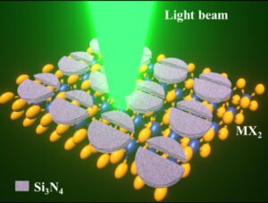 |
Anuj Kumar Singh; Kishor K Mandal; Yashika Gupta; Abhay Anand VS; Lekshmi Eswaramoorthy; Brijesh Kumar; Abhinav Kala; Saurabh Dixit; Venu Gopal Achanta; Anshuman Kumar Low-Cost Plasmonic Platform for Photon-Emission Engineering of Two-Dimensional Semiconductors Journal Article In: Physical Review Applied, vol. 19, no. 4, pp. 044012, 2023. @article{PhysRevApplied.19.044012,
title = {Low-Cost Plasmonic Platform for Photon-Emission Engineering of Two-Dimensional Semiconductors},
author = {Anuj Kumar Singh and Kishor K Mandal and Yashika Gupta and Abhay Anand VS and Lekshmi Eswaramoorthy and Brijesh Kumar and Abhinav Kala and Saurabh Dixit and Venu Gopal Achanta and Anshuman Kumar},
url = {https://doi.org/10.1103/PhysRevApplied.19.044012},
doi = {10.1103/PhysRevApplied.19.044012},
year = {2023},
date = {2023-04-05},
urldate = {2023-04-05},
journal = {Physical Review Applied},
volume = {19},
number = {4},
pages = {044012},
abstract = {Although the field of 2D materials has democratized materials science by making high quality samples accessible cheaply, due to the atomically thin nature of these systems, an integration with nanostructures is almost always required to obtain a significant optical response. Traditionally, these nanostructures are fabricated via electron beam lithography or focused ion beam milling, which are expensive and large area fabrication can be further time consuming. In order to overcome this problem, we report the integration of 2D semiconductors on a cost-effective and large area fabricated nanocone platform. We show that the plasmon modes of our nanocone structures lead to photoluminescence (PL) enhancement of monolayer WSe2 by about eight to ten times compared to the non-plasmonic case, consistent with finite-difference time-domain simulations. Excitation power-dependent measurements reveal that our nanocone platform enables a versatile route to engineering the relative exciton trion contributions to the emission.},
keywords = {},
pubstate = {published},
tppubtype = {article}
}
Although the field of 2D materials has democratized materials science by making high quality samples accessible cheaply, due to the atomically thin nature of these systems, an integration with nanostructures is almost always required to obtain a significant optical response. Traditionally, these nanostructures are fabricated via electron beam lithography or focused ion beam milling, which are expensive and large area fabrication can be further time consuming. In order to overcome this problem, we report the integration of 2D semiconductors on a cost-effective and large area fabricated nanocone platform. We show that the plasmon modes of our nanocone structures lead to photoluminescence (PL) enhancement of monolayer WSe2 by about eight to ten times compared to the non-plasmonic case, consistent with finite-difference time-domain simulations. Excitation power-dependent measurements reveal that our nanocone platform enables a versatile route to engineering the relative exciton trion contributions to the emission. | 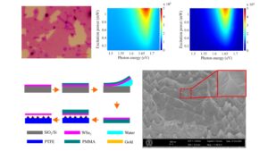 |
Kishor Kumar Mandal; Yashika Gupta; Brijesh Kumar; Mandar Sohoni; Achanta Venu Gopal; Anshuman Kumar A photonic integrated chip platform for interlayer exciton valley routing Journal Article In: Journal of Applied Physics, vol. 133, no. 12, pp. 123104, 2023. @article{doi:10.1063/5.0139880,
title = {A photonic integrated chip platform for interlayer exciton valley routing},
author = {Kishor Kumar Mandal and Yashika Gupta and Brijesh Kumar and Mandar Sohoni and Achanta Venu Gopal and Anshuman Kumar},
url = {https://doi.org/10.1063/5.0139880},
doi = {10.1063/5.0139880},
year = {2023},
date = {2023-03-30},
urldate = {2023-03-30},
journal = {Journal of Applied Physics},
volume = {133},
number = {12},
pages = {123104},
abstract = {Interlayer excitons in two-dimensional semiconductor heterostructures show suppressed electron–hole overlap resulting in longer radiative lifetimes as compared to intralayer excitons. Such tightly bound interlayer excitons are relevant for important optoelectronic applications, including light storage and quantum communication. Their optical accessibility is, however, limited due to their out-of-plane transition dipole moment. In this work, we design a complementary metal–oxide–semiconductor-compatible photonic integrated chip platform for enhanced near-field coupling of these interlayer excitons with the whispering gallery modes of a microresonator, exploiting the high confinement of light in a small modal volume and high-quality factor of the system. Our platform allows for highly selective emission routing via engineering an asymmetric light transmission that facilitates efficient readout and channeling of the excitonic valley state from such systems.
},
keywords = {},
pubstate = {published},
tppubtype = {article}
}
Interlayer excitons in two-dimensional semiconductor heterostructures show suppressed electron–hole overlap resulting in longer radiative lifetimes as compared to intralayer excitons. Such tightly bound interlayer excitons are relevant for important optoelectronic applications, including light storage and quantum communication. Their optical accessibility is, however, limited due to their out-of-plane transition dipole moment. In this work, we design a complementary metal–oxide–semiconductor-compatible photonic integrated chip platform for enhanced near-field coupling of these interlayer excitons with the whispering gallery modes of a microresonator, exploiting the high confinement of light in a small modal volume and high-quality factor of the system. Our platform allows for highly selective emission routing via engineering an asymmetric light transmission that facilitates efficient readout and channeling of the excitonic valley state from such systems.
| 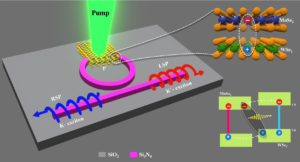 |
Mihir Kumar Sahoo; Abhay Anand VS; Anshuman Kumar Electroplating based engineering of plasmonic nanorod metamaterials for biosensing applications Journal Article In: Nanotechnology, vol. 34, no. 19, pp. 195301, 2023. @article{arXiv:2211.10361,
title = {Electroplating based engineering of plasmonic nanorod metamaterials for biosensing applications},
author = {Mihir Kumar Sahoo and Abhay Anand VS and Anshuman Kumar},
url = {https://doi.org/10.1088/1361-6528/acb948},
doi = {10.1088/1361-6528/acb948},
year = {2023},
date = {2023-02-24},
journal = {Nanotechnology},
volume = {34},
number = {19},
pages = {195301},
abstract = {Sensing lower molecular weight in a diluted solution using a label-free biosensor is challenging and requires a miniaturized plasmonic structure, e.g., a vertical Au nanorod (AuNR) array based metamaterials. The sensitivity of a sensor mainly depends on transducer properties and hence for instance, the AuNR array geometry requires optimization. Physical vapour deposition methods (e.g., sputtering and e-beam evaporation) require a vacuum environment to deposit Au, which is costly, time-consuming, and thickness-limited. On the other hand, chemical deposition, i.e., electroplating deposit higher thickness in less time and at lower cost, becomes an alternative method for Au deposition. In this work, we present a detailed optimization for electroplating based fabrication of these metamaterials. We find that slightly acidic (6.0 < pH < 7.0) gold sulfite solution supports immersion deposition, which should be minimized to avoid uncontrolled Au deposition. Immersion deposition leads to plate-like (for smaller radius AuNR) or capped-like, i.e., mushroom (for higher radius AuNR) structure formation. The electroplating time and DC supply are the tuning parameters that decide the geometry of the vertically aligned AuNR array in area-dependent electroplating deposition. This work will have implications for developing plasmonic metamaterial based sensors.},
keywords = {},
pubstate = {published},
tppubtype = {article}
}
Sensing lower molecular weight in a diluted solution using a label-free biosensor is challenging and requires a miniaturized plasmonic structure, e.g., a vertical Au nanorod (AuNR) array based metamaterials. The sensitivity of a sensor mainly depends on transducer properties and hence for instance, the AuNR array geometry requires optimization. Physical vapour deposition methods (e.g., sputtering and e-beam evaporation) require a vacuum environment to deposit Au, which is costly, time-consuming, and thickness-limited. On the other hand, chemical deposition, i.e., electroplating deposit higher thickness in less time and at lower cost, becomes an alternative method for Au deposition. In this work, we present a detailed optimization for electroplating based fabrication of these metamaterials. We find that slightly acidic (6.0 < pH < 7.0) gold sulfite solution supports immersion deposition, which should be minimized to avoid uncontrolled Au deposition. Immersion deposition leads to plate-like (for smaller radius AuNR) or capped-like, i.e., mushroom (for higher radius AuNR) structure formation. The electroplating time and DC supply are the tuning parameters that decide the geometry of the vertically aligned AuNR array in area-dependent electroplating deposition. This work will have implications for developing plasmonic metamaterial based sensors. | 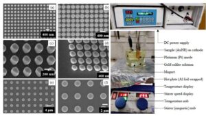 |
2022
|
Yashika Gupta; Anuj K. Singh; Abhay Anand V. S.; Anshuman Kumar Plasmonic nanocavity enhanced luminescence for in-plane and out-of-plane excitons in BA2PbI4 Ruddlesden Popper perovskite thin film Journal Article In: MRS Advances, 2022. @article{Yashika_MRS,
title = {Plasmonic nanocavity enhanced luminescence for in-plane and out-of-plane excitons in BA2PbI4 Ruddlesden Popper perovskite thin film},
author = {Yashika Gupta and Anuj K. Singh and Abhay Anand V. S. and Anshuman Kumar},
url = {https://doi.org/10.1557/s43580-022-00272-9},
doi = {10.1557/s43580-022-00272-9},
year = {2022},
date = {2022-04-06},
journal = {MRS Advances},
abstract = {In this work, we propose an easy-to-fabricate plasmonic cavity design to enhance luminescence from BA2PbI4 Ruddlesden Popper thin films, which otherwise suffer from a very low quantum yield due to strong exciton-phonon interactions in the lattice. We designed a nanoparticle on mirror plasmonic cavity using 3D-finite-difference time-domain simulations, with perovskite film sandwiched between the two metallic structures yielding a 7-fold local enhancement in photoluminescence for intralayer excitons emitting at 520 nm. The designed cavity also aids the detection of interlayer excitons at 540 nm, for which a huge PL enhancement of more than 1500 times is easily obtained.},
keywords = {},
pubstate = {published},
tppubtype = {article}
}
In this work, we propose an easy-to-fabricate plasmonic cavity design to enhance luminescence from BA2PbI4 Ruddlesden Popper thin films, which otherwise suffer from a very low quantum yield due to strong exciton-phonon interactions in the lattice. We designed a nanoparticle on mirror plasmonic cavity using 3D-finite-difference time-domain simulations, with perovskite film sandwiched between the two metallic structures yielding a 7-fold local enhancement in photoluminescence for intralayer excitons emitting at 520 nm. The designed cavity also aids the detection of interlayer excitons at 540 nm, for which a huge PL enhancement of more than 1500 times is easily obtained. | 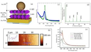 |
Aneesh Bapat; Saurabh Dixit; Yashika Gupta; Tony Low; Anshuman Kumar Gate tunable light-matter interaction in natural biaxial hyperbolic van der Waals heterostructures Journal Article In: Nanophotonics, 2022. @article{arXiv:2110.07526,
title = {Gate tunable light-matter interaction in natural biaxial hyperbolic van der Waals heterostructures},
author = {Aneesh Bapat and Saurabh Dixit and Yashika Gupta and Tony Low and Anshuman Kumar},
url = {https://doi.org/10.1515/nanoph-2022-0034},
doi = {10.1515/nanoph-2022-0034},
year = {2022},
date = {2022-04-04},
urldate = {2022-04-04},
journal = {Nanophotonics},
abstract = {The recent discovery of natural biaxial hyperbolicity in van der Waals crystals, such as α-MoO3, has opened up new avenues for mid-IR nanophotonics due to their deep subwavelength phonon polaritons. However, a significant challenge is the lack of active tunability of these hyperbolic phonon polaritons. In this work, we investigate heterostructures of graphene and α-MoO3 for actively tunable hybrid plasmon phonon polariton modes via electrostatic gating in the mid-infrared spectral region. We observe a unique propagation direction dependent hybridization of graphene plasmon polaritons with hyperbolic phonon polaritons for experimentally feasible values of graphene chemical potential. We further report an application to tunable valley quantum interference in this system with a broad operational bandwidth due to the formation of these hybrid modes. This work presents a lithography-free alternative for actively tunable, anisotropic spontaneous emission enhancement using a sub-wavelength thick naturally biaxial hyperbolic material.},
keywords = {},
pubstate = {published},
tppubtype = {article}
}
The recent discovery of natural biaxial hyperbolicity in van der Waals crystals, such as α-MoO3, has opened up new avenues for mid-IR nanophotonics due to their deep subwavelength phonon polaritons. However, a significant challenge is the lack of active tunability of these hyperbolic phonon polaritons. In this work, we investigate heterostructures of graphene and α-MoO3 for actively tunable hybrid plasmon phonon polariton modes via electrostatic gating in the mid-infrared spectral region. We observe a unique propagation direction dependent hybridization of graphene plasmon polaritons with hyperbolic phonon polaritons for experimentally feasible values of graphene chemical potential. We further report an application to tunable valley quantum interference in this system with a broad operational bandwidth due to the formation of these hybrid modes. This work presents a lithography-free alternative for actively tunable, anisotropic spontaneous emission enhancement using a sub-wavelength thick naturally biaxial hyperbolic material. | 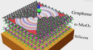 |
Lekshmi Eswaramoorthy; Sudha Mokkapati; Anshuman Kumar Engineering Purcell factor anisotropy for dark and bright excitons in two dimensional semiconductors Journal Article In: Journal of Physics D: Applied Physics, 2022. @article{arXiv:2108.10680,
title = {Engineering Purcell factor anisotropy for dark and bright excitons in two dimensional semiconductors},
author = {Lekshmi Eswaramoorthy and Sudha Mokkapati and Anshuman Kumar},
url = {https://doi.org/10.1088/1361-6463/ac570e},
doi = {10.1088/1361-6463/ac570e},
year = {2022},
date = {2022-02-21},
urldate = {2022-02-21},
journal = {Journal of Physics D: Applied Physics},
abstract = {Tightly bound dark excitons in atomically thin semiconductors can be used for various optoelectronic applications including light storage and quantum communication. Their optical accessibility is however limited due to their out-of-plane transition dipole moment. We thus propose to strengthen the coupling of dark excitons in two dimensional materials with out-of-plane resonant modes of a cavity at room temperature, by engineering the anisotropy in the Purcell factor. A silica micro-disk characterised by high confinement of light in small modal volume, high Q-factor and free spectral range is used to couple to the excitons in monolayer transition metal dichalcogenides. We show numerically that the tapering of sidewalls of the micro-disk is an extremely versatile route for achieving the selective coupling of whispering gallery modes to light emitted from out-of-plane dipoles to the detriment of that from in-plane ones for four representative monolayer transition metal dichalcogenides.},
keywords = {},
pubstate = {published},
tppubtype = {article}
}
Tightly bound dark excitons in atomically thin semiconductors can be used for various optoelectronic applications including light storage and quantum communication. Their optical accessibility is however limited due to their out-of-plane transition dipole moment. We thus propose to strengthen the coupling of dark excitons in two dimensional materials with out-of-plane resonant modes of a cavity at room temperature, by engineering the anisotropy in the Purcell factor. A silica micro-disk characterised by high confinement of light in small modal volume, high Q-factor and free spectral range is used to couple to the excitons in monolayer transition metal dichalcogenides. We show numerically that the tapering of sidewalls of the micro-disk is an extremely versatile route for achieving the selective coupling of whispering gallery modes to light emitted from out-of-plane dipoles to the detriment of that from in-plane ones for four representative monolayer transition metal dichalcogenides. | 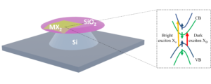 |
Yashika Gupta, Sudharm Rathore, Aparna Singh, Anshuman Kumar Tailoring the mechanical response of Ruddlesden Popper lead halide perovskites Journal Article In: Journal of Alloys and Compounds, vol. 901, pp. 163575, 2022, ISSN: 0925-8388. @article{GUPTA2022163575,
title = {Tailoring the mechanical response of Ruddlesden Popper lead halide perovskites},
author = {Yashika Gupta, Sudharm Rathore, Aparna Singh, Anshuman Kumar},
url = {https://www.sciencedirect.com/science/article/pii/S0925838821049859},
doi = {10.1016/j.jallcom.2021.163575},
issn = {0925-8388},
year = {2022},
date = {2022-01-05},
journal = {Journal of Alloys and Compounds},
volume = {901},
pages = {163575},
abstract = {Two dimensional (2D) Ruddlesden Popper perovskites have been extensively studied for their exceptional optical and electronic characteristics while only a few studies have shed light on their mechanical properties. The existing literature mainly discusses the mechanical strength of single crystal perovskites, however a study of structure tunability of 2D perovskite thin films is still missing. In this study, we report the effect of number of inorganic layers ‘n’ on elastic modulus of 2D, quasi-2D perovskites and 3D perovskite thin films using nanoindentation technique. Our studies indicate the role of orientation of the inorganic layers in perovskite films in tailoring their mechanical response. The experimental results have been substantiated using first principle density functional theory (DFT) calculations. We also report other important mechanical parameters namely, shear modulus, bulk modulus, Poisson’s ratio, Pugh’s ratio, Vickers hardness, yield strength and the universal elastic anisotropic index using DFT simulations. Anisotropy is observed in the elastic modulus of the materials under study and has been discussed in detail in the manuscript. Understanding the mechanical behaviour of 2D Ruddlesden Popper perovskites thin film in comparison with conventional 3D perovskite offers intriguing insights into the atomic layer dependent properties and paves the path for next generation mechanically durable and novel devices.},
keywords = {},
pubstate = {published},
tppubtype = {article}
}
Two dimensional (2D) Ruddlesden Popper perovskites have been extensively studied for their exceptional optical and electronic characteristics while only a few studies have shed light on their mechanical properties. The existing literature mainly discusses the mechanical strength of single crystal perovskites, however a study of structure tunability of 2D perovskite thin films is still missing. In this study, we report the effect of number of inorganic layers ‘n’ on elastic modulus of 2D, quasi-2D perovskites and 3D perovskite thin films using nanoindentation technique. Our studies indicate the role of orientation of the inorganic layers in perovskite films in tailoring their mechanical response. The experimental results have been substantiated using first principle density functional theory (DFT) calculations. We also report other important mechanical parameters namely, shear modulus, bulk modulus, Poisson’s ratio, Pugh’s ratio, Vickers hardness, yield strength and the universal elastic anisotropic index using DFT simulations. Anisotropy is observed in the elastic modulus of the materials under study and has been discussed in detail in the manuscript. Understanding the mechanical behaviour of 2D Ruddlesden Popper perovskites thin film in comparison with conventional 3D perovskite offers intriguing insights into the atomic layer dependent properties and paves the path for next generation mechanically durable and novel devices. | 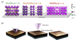 |
2021
|
Yongjun Lee, Johnathas D’arf Severo Forte, Andrey Chaves, Anshuman Kumar, Trang Thu Tran, Youngbum Kim, Shrawan Roy, Takashi Taniguchi, Kenji Watanabe, Alexey Chernikov, Joon I. Jang, Tony Low; Jeongyong Kim Boosting quantum yields in 2D semiconductors via proximal metal plates Journal Article In: Nature Communications, vol. 12, no. 1, pp. 7095, 2021. @article{arXiv:2012.15114,
title = {Boosting quantum yields in 2D semiconductors via proximal metal plates},
author = {Yongjun Lee, Johnathas D’arf Severo Forte, Andrey Chaves, Anshuman Kumar, Trang Thu Tran, Youngbum Kim, Shrawan Roy, Takashi Taniguchi, Kenji Watanabe, Alexey Chernikov, Joon I. Jang, Tony Low and Jeongyong Kim },
url = {https://www.nature.com/articles/s41467-021-27418-x},
doi = {10.1038/s41467-021-27418-x},
year = {2021},
date = {2021-12-07},
urldate = {2021-12-07},
journal = {Nature Communications},
volume = {12},
number = {1},
pages = {7095},
abstract = {Monolayer transition metal dichalcogenides (1L-TMDs) have tremendous potential as atomically thin, direct bandgap semiconductors that can be used as convenient building blocks for quantum photonic devices. However, the short exciton lifetime due to the defect traps and the strong exciton-exciton interaction in TMDs has significantly limited the efficiency of exciton emission from this class of materials. Here, we show that exciton-exciton interaction in 1L-WS2 can be effectively screened using an ultra-flat Au film substrate separated by multilayers of hexagonal boron nitride. Under this geometry, induced dipolar exciton-exciton interaction becomes quadrupole-quadrupole interaction because of effective image dipoles formed within the metal. The suppressed exciton-exciton interaction leads to a significantly improved quantum yield by an order of magnitude, which is also accompanied by a reduction in the exciton-exciton annihilation (EEA) rate, as confirmed by time-resolved optical measurements. A theoretical model accounting for the screening of the dipole-dipole interaction is in a good agreement with the dependence of EEA on exciton densities. Our results suggest that fundamental EEA processes in the TMD can be engineered through proximal metallic screening, which represents a practical approach towards high-efficiency 2D light emitters.},
keywords = {},
pubstate = {published},
tppubtype = {article}
}
Monolayer transition metal dichalcogenides (1L-TMDs) have tremendous potential as atomically thin, direct bandgap semiconductors that can be used as convenient building blocks for quantum photonic devices. However, the short exciton lifetime due to the defect traps and the strong exciton-exciton interaction in TMDs has significantly limited the efficiency of exciton emission from this class of materials. Here, we show that exciton-exciton interaction in 1L-WS2 can be effectively screened using an ultra-flat Au film substrate separated by multilayers of hexagonal boron nitride. Under this geometry, induced dipolar exciton-exciton interaction becomes quadrupole-quadrupole interaction because of effective image dipoles formed within the metal. The suppressed exciton-exciton interaction leads to a significantly improved quantum yield by an order of magnitude, which is also accompanied by a reduction in the exciton-exciton annihilation (EEA) rate, as confirmed by time-resolved optical measurements. A theoretical model accounting for the screening of the dipole-dipole interaction is in a good agreement with the dependence of EEA on exciton densities. Our results suggest that fundamental EEA processes in the TMD can be engineered through proximal metallic screening, which represents a practical approach towards high-efficiency 2D light emitters. | 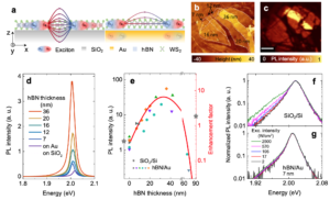 |
Nihar Ranjan Sahoo; Saurabh Dixit; Anuj Kumar Singh; Sang Hoon Nam; Nicholas X. Fang; Anshuman Kumar High temperature mid-IR polarizer via natural in-plane hyperbolic van der Waals crystals Journal Article In: Advanced Optical Materials, pp. 2101919, 2021. @article{arXiv:2108.08510,
title = {High temperature mid-IR polarizer via natural in-plane hyperbolic van der Waals crystals},
author = {Nihar Ranjan Sahoo and Saurabh Dixit and Anuj Kumar Singh and Sang Hoon Nam and Nicholas X. Fang and Anshuman Kumar},
url = {https://onlinelibrary.wiley.com/doi/abs/10.1002/adom.202101919},
doi = {10.1002/adom.202101919},
year = {2021},
date = {2021-12-07},
journal = {Advanced Optical Materials},
pages = {2101919},
abstract = {Integration of conventional mid to long-wavelength infrared polarizers with chip-scale platforms is restricted by their bulky size and complex fabrication. Van der Waals materials based polarizer can address these challenges due to its non-lithographic fabrication, ease of integration with chip-scale platforms, and room temperature operation. In the present work, mid-IR optical response of the sub-wavelength thin films of α-MoO3 is investigated for application towards high temperature mid-IR transmission and reflection type thin film polarizer. To our knowledge, this is the first report of above room temperature mid-IR optical response of α-MoO3 to determine the thermal stability of the proposed device. We find that our α-MoO3 based polarizer retains high extinction ratio with peak value exceeding 10 dB, up to a temperature of 140∘C. We explain our experimental findings by natural in-plane hyperbolic anisotropy of α-MoO3 in the mid-IR, high temperature X-ray diffraction and Raman spectroscopic measurements. This work opens up new avenues for naturally in-plane hyperbolic van der Waals thin-films to realize sub-wavelength IR optical components without lithographic constraints.},
keywords = {},
pubstate = {published},
tppubtype = {article}
}
Integration of conventional mid to long-wavelength infrared polarizers with chip-scale platforms is restricted by their bulky size and complex fabrication. Van der Waals materials based polarizer can address these challenges due to its non-lithographic fabrication, ease of integration with chip-scale platforms, and room temperature operation. In the present work, mid-IR optical response of the sub-wavelength thin films of α-MoO3 is investigated for application towards high temperature mid-IR transmission and reflection type thin film polarizer. To our knowledge, this is the first report of above room temperature mid-IR optical response of α-MoO3 to determine the thermal stability of the proposed device. We find that our α-MoO3 based polarizer retains high extinction ratio with peak value exceeding 10 dB, up to a temperature of 140∘C. We explain our experimental findings by natural in-plane hyperbolic anisotropy of α-MoO3 in the mid-IR, high temperature X-ray diffraction and Raman spectroscopic measurements. This work opens up new avenues for naturally in-plane hyperbolic van der Waals thin-films to realize sub-wavelength IR optical components without lithographic constraints. | 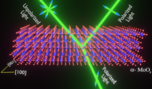 |
Sudharm Rathore; Guifang Han; Anshuman Kumar; Wei Lin Leong; Aparna Singh Elastic modulus tailoring in CH3NH3PbI3 perovskite system by the introduction of two dimensionality using (5-AVA)2PbI4 Journal Article In: Solar Energy, vol. 224, pp. 27-34, 2021, ISSN: 0038-092X. @article{AVA202127,
title = {Elastic modulus tailoring in CH3NH3PbI3 perovskite system by the introduction of two dimensionality using (5-AVA)2PbI4},
author = {Sudharm Rathore and Guifang Han and Anshuman Kumar and Wei Lin Leong and Aparna Singh},
url = {https://www.sciencedirect.com/science/article/pii/S0038092X21003911},
doi = {10.1016/j.solener.2021.05.027},
issn = {0038-092X},
year = {2021},
date = {2021-06-04},
journal = {Solar Energy},
volume = {224},
pages = {27-34},
abstract = {The stiffness of the perovskite active layer plays a critical role in influencing the flexibility of a solar cell. This is one of the important parameters which must be considered while deciding the architecture of the flexible device. Till now, there have been limited studies on the mechanical properties of 2D and 3D perovskite thin films. In this study, we report the very first time, the elastic modulus of the most commonly used 3D perovskite i.e. methylammonium lead iodide (MaPbI3), the pure 2D perovskite (5-AVA)2PbI4 which is based on 5-aminovaleric acid (5-AVA) cation as well as the 2D-3D mixed perovskites thin films through nanoindentation technique. The elastic modulus for the 3D perovskite has been found to be around 16.5 GPa, while it decreases to 6.3 GPa for pure 2D perovskite. The experimental results have also been corroborated by density functional theory calculations done for the 2D and 3D perovskite. The 2D perovskite shows a much lower modulus than the 3D perovskite and can be used within a 2D-3D mixture for improving the mechanical flexibility of the active layer. Also, it is well established that 2D perovskites are much more stable against moisture as compared to their 3D counterparts due to the presence of hydrophobic organic alkyl ammonium cation. Thus, the device containing an active layer comprising of a mixture of 3D and 2D perovskite can be used to improve the environmental stability of the overall device in addition to achieving mechanical durability.},
keywords = {},
pubstate = {published},
tppubtype = {article}
}
The stiffness of the perovskite active layer plays a critical role in influencing the flexibility of a solar cell. This is one of the important parameters which must be considered while deciding the architecture of the flexible device. Till now, there have been limited studies on the mechanical properties of 2D and 3D perovskite thin films. In this study, we report the very first time, the elastic modulus of the most commonly used 3D perovskite i.e. methylammonium lead iodide (MaPbI3), the pure 2D perovskite (5-AVA)2PbI4 which is based on 5-aminovaleric acid (5-AVA) cation as well as the 2D-3D mixed perovskites thin films through nanoindentation technique. The elastic modulus for the 3D perovskite has been found to be around 16.5 GPa, while it decreases to 6.3 GPa for pure 2D perovskite. The experimental results have also been corroborated by density functional theory calculations done for the 2D and 3D perovskite. The 2D perovskite shows a much lower modulus than the 3D perovskite and can be used within a 2D-3D mixture for improving the mechanical flexibility of the active layer. Also, it is well established that 2D perovskites are much more stable against moisture as compared to their 3D counterparts due to the presence of hydrophobic organic alkyl ammonium cation. Thus, the device containing an active layer comprising of a mixture of 3D and 2D perovskite can be used to improve the environmental stability of the overall device in addition to achieving mechanical durability. | 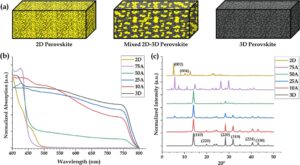 |
Saurabh Dixit, Nihar Ranjan Sahoo, Abhishek Mall, Anshuman Kumar Mid infrared polarization engineering via sub-wavelength biaxial hyperbolic van der Waals crystals Journal Article In: Scientific Reports, vol. 11, no. 1, pp. 6612, 2021. @article{arXiv:2007.11265,
title = {Mid infrared polarization engineering via sub-wavelength biaxial hyperbolic van der Waals crystals},
author = {Saurabh Dixit, Nihar Ranjan Sahoo, Abhishek Mall, Anshuman Kumar},
url = {https://www.nature.com/articles/s41598-021-86056-x},
doi = {10.1038/s41598-021-86056-x},
year = {2021},
date = {2021-03-23},
journal = {Scientific Reports},
volume = {11},
number = {1},
pages = {6612},
abstract = {Mid-infrared (IR) spectral region is of immense importance for astronomy, medical diagnosis, security and imaging due to the existence of the vibrational modes of many important molecules in this spectral range. Therefore, there is a particular interest in miniaturization and integration of IR optical components. To this end, 2D van der Waals (vdW) crystals have shown great potential owing to their ease of integration with other optoelectronic platforms and room temperature operation. Recently, 2D vdW crystals of α-MoO3 and α-V2O5 have been shown to possess the unique phenomenon of natural in-plane biaxial hyperbolicity in the mid-infrared frequency regime at room temperature. Here, we report a unique application of this in-plane hyperbolicity for designing highly efficient, lithography free and extremely subwavelength mid-IR photonic devices for polarization engineering. In particular, we show the possibility of a significant reduction in the device footprint while maintaining an enormous extinction ratio from α-MoO3 and α-V2O5 based mid-IR polarizers. Furthermore, we investigate the application of sub-wavelength thin films of these vdW crystals towards engineering the polarization state of incident mid-IR light via precise control of polarization rotation, ellipticity and relative phase. We explain our results using natural in-plane hyperbolic anisotropy of α-MoO3 and α-V2O5 via both analytical and full-wave electromagnetic simulations. This work provides a lithography free alternative for miniaturized mid-infrared photonic devices using the hyperbolic anisotropy of α-MoO3 and α-V2O5.},
keywords = {},
pubstate = {published},
tppubtype = {article}
}
Mid-infrared (IR) spectral region is of immense importance for astronomy, medical diagnosis, security and imaging due to the existence of the vibrational modes of many important molecules in this spectral range. Therefore, there is a particular interest in miniaturization and integration of IR optical components. To this end, 2D van der Waals (vdW) crystals have shown great potential owing to their ease of integration with other optoelectronic platforms and room temperature operation. Recently, 2D vdW crystals of α-MoO3 and α-V2O5 have been shown to possess the unique phenomenon of natural in-plane biaxial hyperbolicity in the mid-infrared frequency regime at room temperature. Here, we report a unique application of this in-plane hyperbolicity for designing highly efficient, lithography free and extremely subwavelength mid-IR photonic devices for polarization engineering. In particular, we show the possibility of a significant reduction in the device footprint while maintaining an enormous extinction ratio from α-MoO3 and α-V2O5 based mid-IR polarizers. Furthermore, we investigate the application of sub-wavelength thin films of these vdW crystals towards engineering the polarization state of incident mid-IR light via precise control of polarization rotation, ellipticity and relative phase. We explain our results using natural in-plane hyperbolic anisotropy of α-MoO3 and α-V2O5 via both analytical and full-wave electromagnetic simulations. This work provides a lithography free alternative for miniaturized mid-infrared photonic devices using the hyperbolic anisotropy of α-MoO3 and α-V2O5. | 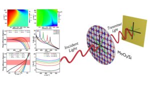 |
2020
|
Abhishek Mall, Abhijeet Patil, Amit Sethi, Anshuman Kumar A Cyclical Deep Learning Based Framework For Simultaneous Inverse and Forward design of Nanophotonic Metasurfaces Journal Article In: Scientific Reports, vol. 10, no. 1, pp. 19427, 2020. @article{arXiv:2005.12796,
title = {A Cyclical Deep Learning Based Framework For Simultaneous Inverse and Forward design of Nanophotonic Metasurfaces},
author = {Abhishek Mall, Abhijeet Patil, Amit Sethi, Anshuman Kumar},
url = {https://www.nature.com/articles/s41598-020-76400-y},
doi = {10.1038/s41598-020-76400-y},
year = {2020},
date = {2020-11-10},
urldate = {2020-11-10},
journal = {Scientific Reports},
volume = {10},
number = {1},
pages = {19427},
abstract = {The conventional approach to nanophotonic metasurface design and optimization for a targeted electromagnetic response involves exploring large geometry and material spaces. This is a highly iterative process based on trial and error, which is computationally costly and time consuming. Moreover, the non-uniqueness of structural designs and high non-linearity between electromagnetic response and design makes this problem challenging. To model this unintuitive relationship between electromagnetic response and metasurface structural design as a probability distribution in the design space, we introduce a framework for inverse design of nanophotonic metasurfaces based on cyclical deep learning (DL). The proposed framework performs inverse design and optimization mechanism for the generation of meta-atoms and meta-molecules as metasurface units based on DL models and genetic algorithm. The framework includes consecutive DL models that emulate both numerical electromagnetic simulation and iterative processes of optimization, and generate optimized structural designs while simultaneously performing forward and inverse design tasks. A selection and evaluation of generated structural designs is performed by the genetic algorithm to construct a desired optical response and design space that mimics real world responses. Importantly, our cyclical generation framework also explores the space of new metasurface topologies. As an example application of the utility of our proposed architecture, we demonstrate the inverse design of gap-plasmon based half-wave plate metasurface for user-defined optical response. Our proposed technique can be easily generalized for designing nanophtonic metasurfaces for a wide range of targeted optical response.},
keywords = {},
pubstate = {published},
tppubtype = {article}
}
The conventional approach to nanophotonic metasurface design and optimization for a targeted electromagnetic response involves exploring large geometry and material spaces. This is a highly iterative process based on trial and error, which is computationally costly and time consuming. Moreover, the non-uniqueness of structural designs and high non-linearity between electromagnetic response and design makes this problem challenging. To model this unintuitive relationship between electromagnetic response and metasurface structural design as a probability distribution in the design space, we introduce a framework for inverse design of nanophotonic metasurfaces based on cyclical deep learning (DL). The proposed framework performs inverse design and optimization mechanism for the generation of meta-atoms and meta-molecules as metasurface units based on DL models and genetic algorithm. The framework includes consecutive DL models that emulate both numerical electromagnetic simulation and iterative processes of optimization, and generate optimized structural designs while simultaneously performing forward and inverse design tasks. A selection and evaluation of generated structural designs is performed by the genetic algorithm to construct a desired optical response and design space that mimics real world responses. Importantly, our cyclical generation framework also explores the space of new metasurface topologies. As an example application of the utility of our proposed architecture, we demonstrate the inverse design of gap-plasmon based half-wave plate metasurface for user-defined optical response. Our proposed technique can be easily generalized for designing nanophtonic metasurfaces for a wide range of targeted optical response. | 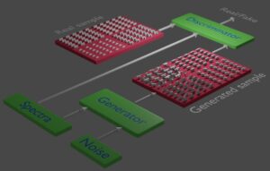 |
Mandar Sohoni, Pankaj K. Jha, Muralidhar Nalabothula, Anshuman Kumar Interlayer Exciton Valleytronics in Bilayer Heterostructures Interfaced with a Metasurface Journal Article In: Applied Physics Letters, vol. 117, no. 12, pp. 121101, 2020. @article{arXiv:1912.12080,
title = {Interlayer Exciton Valleytronics in Bilayer Heterostructures Interfaced with a Metasurface},
author = {Mandar Sohoni, Pankaj K. Jha, Muralidhar Nalabothula, Anshuman Kumar},
url = {https://doi.org/10.1063/5.0015087},
doi = {10.1063/5.0015087},
year = {2020},
date = {2020-09-21},
urldate = {2020-09-21},
journal = {Applied Physics Letters},
volume = {117},
number = {12},
pages = {121101},
abstract = {The recent proposal of using an anisotropic vacuum for generating valley coherence in transition metal dichalcogenide (TMDC) monolayers has expanded the potential of such valley degrees of freedom for applications in valleytronics. In this work, we open up a completely new regime, inaccessible with monolayer TMDCs, of spontaneously generated valley coherence in interlayer excitons in commensurate TMDC bilayer heterostructures. Using the peculiar out of plane polarization of interlayer excitons in conjunction with an in-plane anisotropic electromagnetic vacuum, we show that a much larger region of the Bloch sphere can be accessible in these heterostructures. We show the accessible phases of these excitons given this in-plane anisotropic electromagnetic vacuum. Our analysis of spontaneous coherence for interlayer excitons may pave the way for engineering an array of interacting quantum emitters in Moiré heterostructures.},
keywords = {},
pubstate = {published},
tppubtype = {article}
}
The recent proposal of using an anisotropic vacuum for generating valley coherence in transition metal dichalcogenide (TMDC) monolayers has expanded the potential of such valley degrees of freedom for applications in valleytronics. In this work, we open up a completely new regime, inaccessible with monolayer TMDCs, of spontaneously generated valley coherence in interlayer excitons in commensurate TMDC bilayer heterostructures. Using the peculiar out of plane polarization of interlayer excitons in conjunction with an in-plane anisotropic electromagnetic vacuum, we show that a much larger region of the Bloch sphere can be accessible in these heterostructures. We show the accessible phases of these excitons given this in-plane anisotropic electromagnetic vacuum. Our analysis of spontaneous coherence for interlayer excitons may pave the way for engineering an array of interacting quantum emitters in Moiré heterostructures. | 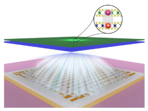 |
Feliciano Giustino; Manuel Bibes; Jin Hong Lee; Felix Trier; Roser Valentí; Stephen M. Winter; Young-Woo Son; Louis Taillefer; Christoph Heil; Adriana I. Figueroa; Bernard Plaçais; QuanSheng Wu; Oleg V Yazyev; Erik P A M Bakkers; Jesper Nygård; Pol Forn-Díaz; Silvano de Franceschi; Luis E. F. Foa Torres; James McIver; Anshuman Kumar; Tony Low; Regina Galceran; Sergio O. Valenzuela; Marius Vasile Costache; Aurélien Manchon; Eun-Ah Kim; Gabriel Ravanhani Schleder; Adalberto Fazzio; Stephan Roche The 2020 Quantum Materials Roadmap Journal Article In: Journal of Physics: Materials, 2020. @article{quantum_Materials_Roadmap,
title = {The 2020 Quantum Materials Roadmap},
author = {Feliciano Giustino and Manuel Bibes and Jin Hong Lee and Felix Trier and Roser Valentí and Stephen M. Winter and Young-Woo Son and Louis Taillefer and Christoph Heil and Adriana I. Figueroa and Bernard Plaçais and QuanSheng Wu and Oleg V Yazyev and Erik P A M Bakkers and Jesper Nygård and Pol Forn-Díaz and Silvano de Franceschi and Luis E. F. Foa Torres and James McIver and Anshuman Kumar and Tony Low and Regina Galceran and Sergio O. Valenzuela and Marius Vasile Costache and Aurélien Manchon and Eun-Ah Kim and Gabriel Ravanhani Schleder and Adalberto Fazzio and Stephan Roche},
url = {https://doi.org/10.1088/2515-7639/abb74e},
doi = {10.1088/2515-7639/abb74e},
year = {2020},
date = {2020-09-10},
urldate = {2020-09-10},
journal = {Journal of Physics: Materials},
keywords = {},
pubstate = {published},
tppubtype = {article}
}
| 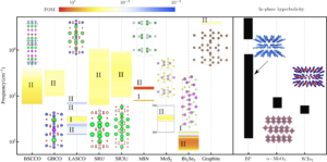 |
Abhishek Mall, Abhijeet Patil, Dipesh Tamboli, Amit Sethi, Anshuman Kumar Fast Design of Plasmonic Metasurfaces Enabled by Deep Learning Journal Article In: Journal of Physics D: Applied Physics, vol. 53, no. 49, pp. 49LT01, 2020. @article{arXiv:2003.12402,
title = {Fast Design of Plasmonic Metasurfaces Enabled by Deep Learning},
author = {Abhishek Mall, Abhijeet Patil, Dipesh Tamboli, Amit Sethi, Anshuman Kumar},
url = {https://doi.org/10.1088/1361-6463/abb33c},
doi = {10.1088/1361-6463/abb33c},
year = {2020},
date = {2020-08-27},
urldate = {2020-08-27},
journal = {Journal of Physics D: Applied Physics},
volume = {53},
number = {49},
pages = {49LT01},
abstract = {Metasurfaces is an emerging field that enables the manipulation of light by an ultrathin structure composed of subwavelength antennae and fulfills an important requirement for miniaturized optical elements. Finding a new design for a metasurface or optimizing an existing design for a desired functionality is a computationally expensive and time consuming process as it is based on an iterative process of trial and error. We propose a deep learning (DL) architecture dubbed bidirectional autoencoder for nanophotonic metasurface design via a template search methodology. In contrast with the earlier approaches based on DL, our methodology addresses optimization in the space of multiple metasurface topologies instead of just one, in order to tackle the one to many mapping problem of inverse design. We demonstrate the creation of a Geometry and Parameter Space Library (GPSL) of metasurface designs with their corresponding optical response using our DL model. This GPSL acts as a universal design and response space for the optimization. As an example application, we use our methodology to design a multi-band gap-plasmon based half-wave plate metasurface. Through this example, we demonstrate the power of our technique in addressing the nonuniqueness problem of common inverse design approaches by showing that our network converges aptly to multiple metasurface topologies for the desired optical response. Our proposed technique would enable fast and accurate design and optimization of various kinds of metasurfaces with different functionalities.},
keywords = {},
pubstate = {published},
tppubtype = {article}
}
Metasurfaces is an emerging field that enables the manipulation of light by an ultrathin structure composed of subwavelength antennae and fulfills an important requirement for miniaturized optical elements. Finding a new design for a metasurface or optimizing an existing design for a desired functionality is a computationally expensive and time consuming process as it is based on an iterative process of trial and error. We propose a deep learning (DL) architecture dubbed bidirectional autoencoder for nanophotonic metasurface design via a template search methodology. In contrast with the earlier approaches based on DL, our methodology addresses optimization in the space of multiple metasurface topologies instead of just one, in order to tackle the one to many mapping problem of inverse design. We demonstrate the creation of a Geometry and Parameter Space Library (GPSL) of metasurface designs with their corresponding optical response using our DL model. This GPSL acts as a universal design and response space for the optimization. As an example application, we use our methodology to design a multi-band gap-plasmon based half-wave plate metasurface. Through this example, we demonstrate the power of our technique in addressing the nonuniqueness problem of common inverse design approaches by showing that our network converges aptly to multiple metasurface topologies for the desired optical response. Our proposed technique would enable fast and accurate design and optimization of various kinds of metasurfaces with different functionalities. | 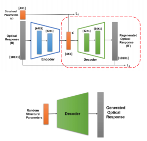 |
Muralidhar Nalabothula, Pankaj Jha, Tony Low, Anshuman Kumar Engineering valley quantum interference in anisotropic van der Waals heterostructures Journal Article In: Phys. Rev. B, vol. 102, no. 4, pp. 045416, 2020. @article{PhysRevB.102.045416,
title = {Engineering valley quantum interference in anisotropic van der Waals heterostructures},
author = {Muralidhar Nalabothula, Pankaj Jha, Tony Low, Anshuman Kumar},
url = {https://link.aps.org/doi/10.1103/PhysRevB.102.045416},
doi = {10.1103/PhysRevB.102.045416},
year = {2020},
date = {2020-07-15},
journal = {Phys. Rev. B},
volume = {102},
number = {4},
pages = {045416},
abstract = {In this paper, we present a novel route to manipulate the spontaneous valley coherence in two-dimensional valleytronic materials interfaced with other layered materials hosting anisotropic polaritonic modes. We propose two implementations — one, using anisotropic plasmons in phosphorene and another with hyperbolic phonon polaritons in MoO3. In particular, we show the electrostatic tunability of the spontaneous valley coherence achieving robust valley coherence values in the near-infrared wavelengths at room temperature. The tunability of this valley coherence shown in these heterostructures would enable the realization of active valleytronic quantum circuitry.},
keywords = {},
pubstate = {published},
tppubtype = {article}
}
In this paper, we present a novel route to manipulate the spontaneous valley coherence in two-dimensional valleytronic materials interfaced with other layered materials hosting anisotropic polaritonic modes. We propose two implementations — one, using anisotropic plasmons in phosphorene and another with hyperbolic phonon polaritons in MoO3. In particular, we show the electrostatic tunability of the spontaneous valley coherence achieving robust valley coherence values in the near-infrared wavelengths at room temperature. The tunability of this valley coherence shown in these heterostructures would enable the realization of active valleytronic quantum circuitry. | 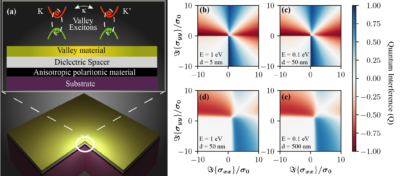 |
2019
|
Edo van Veen, Andrei Nemilentsau, Anshuman Kumar, Rafael Roldan, Mikhail I. Katsnelson, Tony Low; Shengjun Yuan Tuning Two-Dimensional Hyperbolic Plasmons in Black Phosphorus Journal Article In: Phys. Rev. Applied, vol. 12, no. 014011, 2019. @article{BP_hyperbolic,
title = {Tuning Two-Dimensional Hyperbolic Plasmons in Black Phosphorus},
author = {Edo van Veen, Andrei Nemilentsau, Anshuman Kumar, Rafael Roldan, Mikhail I. Katsnelson, Tony Low and Shengjun Yuan},
url = {https://journals.aps.org/prapplied/abstract/10.1103/PhysRevApplied.12.014011},
doi = {10.1103/PhysRevApplied.12.014011},
year = {2019},
date = {2019-07-08},
journal = {Phys. Rev. Applied},
volume = {12},
number = {014011},
abstract = {Black phosphorus presents a very anisotropic crystal structure, making it a potential candidate for hyperbolic plasmonics, characterized by a permittivity tensor where one of the principal components is metallic and the other dielectric. Here we demonstrate that atomically thin black phosphorus can be engineered to be a hyperbolic material operating in a broad range of the electromagnetic spectrum from the entire visible spectrum to ultraviolet. With the introduction of an optical gain, a new hyperbolic region emerges in the infrared. The character of this hyperbolic plasmon depends on the interplay between gain and loss along the two crystalline directions.},
keywords = {},
pubstate = {published},
tppubtype = {article}
}
Black phosphorus presents a very anisotropic crystal structure, making it a potential candidate for hyperbolic plasmonics, characterized by a permittivity tensor where one of the principal components is metallic and the other dielectric. Here we demonstrate that atomically thin black phosphorus can be engineered to be a hyperbolic material operating in a broad range of the electromagnetic spectrum from the entire visible spectrum to ultraviolet. With the introduction of an optical gain, a new hyperbolic region emerges in the infrared. The character of this hyperbolic plasmon depends on the interplay between gain and loss along the two crystalline directions. | 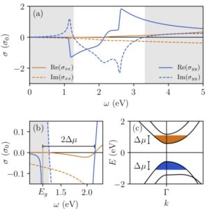 |
2018
|
Yong-Liang Zhang; Raymond P. H. Wu; Anshuman Kumar; Tieyan Si; Kin Hung Fung Nonsymmorphic symmetry-protected topological modes in plasmonic nanoribbon lattices Journal Article In: Phys. Rev. B, vol. 97, no. 144203, 2018. @article{PRB_nonsym,
title = {Nonsymmorphic symmetry-protected topological modes in plasmonic nanoribbon lattices},
author = {Yong-Liang Zhang and Raymond P. H. Wu and Anshuman Kumar and Tieyan Si and Kin Hung Fung},
doi = {10.1103/PhysRevB.97.144203},
year = {2018},
date = {2018-04-20},
journal = {Phys. Rev. B},
volume = {97},
number = {144203},
abstract = {Using a dynamic eigenresponse theory, we study the topological edge plasmon modes in dispersive plasmonic lattices constructed by unit cells of multiple nanoribbons. In dipole approximation, the bulk-edge correspondence in the lattices made of dimerized unit cell and one of its square-root daughter with nonsymmorphic symmetry are demonstrated. Calculations with consideration of dynamic long-range effects and retardation are compared to those given by nearest-neighbor approximations. It is shown that nonsymmorphic symmetry opens up two symmetric gaps where versatile topological edge plasmon modes are found. Unprecedented spectral shifts of the edge states with respect to the zero modes due to long-range coupling are found. The proposed ribbon structure is favorable to electrical gating and thus could serve as an on-chip platform for electrically controllable subwavelength edge states at optical wavelengths. Our eigenresponse approach provides a powerful tool for the radiative topological mode analysis in strongly coupled plasmonic lattices.},
keywords = {},
pubstate = {published},
tppubtype = {article}
}
Using a dynamic eigenresponse theory, we study the topological edge plasmon modes in dispersive plasmonic lattices constructed by unit cells of multiple nanoribbons. In dipole approximation, the bulk-edge correspondence in the lattices made of dimerized unit cell and one of its square-root daughter with nonsymmorphic symmetry are demonstrated. Calculations with consideration of dynamic long-range effects and retardation are compared to those given by nearest-neighbor approximations. It is shown that nonsymmorphic symmetry opens up two symmetric gaps where versatile topological edge plasmon modes are found. Unprecedented spectral shifts of the edge states with respect to the zero modes due to long-range coupling are found. The proposed ribbon structure is favorable to electrical gating and thus could serve as an on-chip platform for electrically controllable subwavelength edge states at optical wavelengths. Our eigenresponse approach provides a powerful tool for the radiative topological mode analysis in strongly coupled plasmonic lattices. |  |
Cl'ement Javerzac-Galy*; Anshuman Kumar*; Ryan D. Schilling; Nicolas Piro; Sina Khorasani; Matteo Barbone; Ilya Goykhman; Jacob B. Khurgin; Andrea C. Ferrari; Tobias J Kippenberg Excitonic emission of monolayer semiconductors near-field coupled to high-Q microresonators Journal Article In: Nano Letters, vol. 18, no. 5, pp. 3138–3146, 2018. @article{NL_EPFL,
title = {Excitonic emission of monolayer semiconductors near-field coupled to high-Q microresonators},
author = {Cl{'e}ment Javerzac-Galy* and Anshuman Kumar* and Ryan D. Schilling and Nicolas Piro and Sina Khorasani and Matteo Barbone and Ilya Goykhman and Jacob B. Khurgin and Andrea C. Ferrari and Tobias J Kippenberg},
doi = {10.1021/acs.nanolett.8b00749},
year = {2018},
date = {2018-04-06},
urldate = {2018-04-06},
journal = {Nano Letters},
volume = {18},
number = {5},
pages = {3138--3146},
abstract = {We present quantum yield measurements of single layer WSe2 (1L-WSe2) integrated with high-Q (Q > 106) optical microdisk cavities, using an efficient (η > 90
keywords = {},
pubstate = {published},
tppubtype = {article}
}
We present quantum yield measurements of single layer WSe2 (1L-WSe2) integrated with high-Q (Q > 106) optical microdisk cavities, using an efficient (η > 90
2017
|
|
Cl'ement Javerzac-Galy; Nicolas Piro; Ryan D. Schilling; Anshuman Kumar; Matteo Barbone; Ilya Goykhman; Andrea C. Ferrari; Tobias J. Kippenberg High-Q optical microresonators functionalized with two-dimensional material Conference Conference on Lasers and Electro-Optics, Optical Society of America Optical Society of America, 2017. @conference{JAVERZAC-GALY:17,
title = {High-Q optical microresonators functionalized with two-dimensional material},
author = {Cl{'e}ment Javerzac-Galy and Nicolas Piro and Ryan D. Schilling and Anshuman Kumar and Matteo Barbone and Ilya Goykhman and Andrea C. Ferrari and Tobias J. Kippenberg},
url = {http://www.osapublishing.org/abstract.cfm?URI=CLEO_SI-2017-STh1I.2},
doi = {10.1364/CLEO_SI.2017.STh1I.2},
year = {2017},
date = {2017-01-01},
urldate = {2017-01-01},
booktitle = {Conference on Lasers and Electro-Optics},
pages = {STh1I.2},
publisher = {Optical Society of America},
organization = {Optical Society of America},
abstract = {We report the functionalization of high-Q silica microdisks with WSe2 and their optical characterization. Background-free cavity enhanced photoluminescence and photoluminescence saturation are observed at room temperature. We show precise measurements of the quantum yield of WSe2.},
keywords = {},
pubstate = {published},
tppubtype = {conference}
}
We report the functionalization of high-Q silica microdisks with WSe2 and their optical characterization. Background-free cavity enhanced photoluminescence and photoluminescence saturation are observed at room temperature. We show precise measurements of the quantum yield of WSe2. |  |
Tony Low; Andrey Chaves; Joshua D. Caldwell; Anshuman Kumar; Nicholas X. Fang; Phaedon Avouris; Tony F. Heinz; Francisco Guinea; Luis Martin-Moreno; Frank Koppens Polaritons in layered two-dimensional materials Journal Article In: Nature Materials, vol. 16, no. 2, pp. 182–194, 2017, ISSN: 1476-1122. @article{low_polaritons_2017,
title = {Polaritons in layered two-dimensional materials},
author = {Tony Low and Andrey Chaves and Joshua D. Caldwell and Anshuman Kumar and Nicholas X. Fang and Phaedon Avouris and Tony F. Heinz and Francisco Guinea and Luis Martin-Moreno and Frank Koppens},
url = {http://www.nature.com/nmat/journal/v16/n2/full/nmat4792.html},
doi = {10.1038/nmat4792},
issn = {1476-1122},
year = {2017},
date = {2017-01-01},
journal = {Nature Materials},
volume = {16},
number = {2},
pages = {182–194},
abstract = {In recent years, enhanced light–matter interactions through a plethora of dipole-type polaritonic excitations have been observed in two-dimensional (2D) layered materials. In graphene, electrically tunable and highly confined plasmon-polaritons were predicted and observed, opening up opportunities for optoelectronics, bio-sensing and other mid-infrared applications. In hexagonal boron nitride, low-loss infrared-active phonon-polaritons exhibit hyperbolic behaviour for some frequencies, allowing for ray-like propagation exhibiting high quality factors and hyperlensing effects. In transition metal dichalcogenides, reduced screening in the 2D limit leads to optically prominent excitons with large binding energy, with these polaritonic modes having been recently observed with scanning near-field optical microscopy. Here, we review recent progress in state-of-the-art experiments, and survey the vast library of polaritonic modes in 2D materials, their optical spectral properties, figures of merit and application space. Taken together, the emerging field of 2D material polaritonics and their hybrids provide enticing avenues for manipulating light–matter interactions across the visible, infrared to terahertz spectral ranges, with new optical control beyond what can be achieved using traditional bulk materials.},
keywords = {},
pubstate = {published},
tppubtype = {article}
}
In recent years, enhanced light–matter interactions through a plethora of dipole-type polaritonic excitations have been observed in two-dimensional (2D) layered materials. In graphene, electrically tunable and highly confined plasmon-polaritons were predicted and observed, opening up opportunities for optoelectronics, bio-sensing and other mid-infrared applications. In hexagonal boron nitride, low-loss infrared-active phonon-polaritons exhibit hyperbolic behaviour for some frequencies, allowing for ray-like propagation exhibiting high quality factors and hyperlensing effects. In transition metal dichalcogenides, reduced screening in the 2D limit leads to optically prominent excitons with large binding energy, with these polaritonic modes having been recently observed with scanning near-field optical microscopy. Here, we review recent progress in state-of-the-art experiments, and survey the vast library of polaritonic modes in 2D materials, their optical spectral properties, figures of merit and application space. Taken together, the emerging field of 2D material polaritonics and their hybrids provide enticing avenues for manipulating light–matter interactions across the visible, infrared to terahertz spectral ranges, with new optical control beyond what can be achieved using traditional bulk materials. |  |
2016
|
Anshuman Kumar; Andrei Nemilentsau; Kin Hung Fung; George Hanson; Nicholas X. Fang; Tony Low Chiral plasmon in gapped Dirac systems Journal Article In: Phys. Rev. B, vol. 93, pp. 041413, 2016. @article{PhysRevB.93.041413,
title = {Chiral plasmon in gapped Dirac systems},
author = {Anshuman Kumar and Andrei Nemilentsau and Kin Hung Fung and George Hanson and Nicholas X. Fang and Tony Low},
url = {http://link.aps.org/doi/10.1103/PhysRevB.93.041413},
doi = {10.1103/PhysRevB.93.041413},
year = {2016},
date = {2016-01-01},
journal = {Phys. Rev. B},
volume = {93},
pages = {041413},
publisher = {American Physical Society},
keywords = {},
pubstate = {published},
tppubtype = {article}
}
|  |
Himanshu Tyagi; Ajay Kushwaha; Anshuman Kumar; Mohammed Aslam A Facile pH Controlled Citrate-Based Reduction Method for Gold Nanoparticle Synthesis at Room Temperature Journal Article In: Nanoscale Research Letters, vol. 11, no. 1, pp. 1–11, 2016, ISSN: 1556-276X. @article{Tyagi2016,
title = {A Facile pH Controlled Citrate-Based Reduction Method for Gold Nanoparticle Synthesis at Room Temperature},
author = {Himanshu Tyagi and Ajay Kushwaha and Anshuman Kumar and Mohammed Aslam},
url = {http://dx.doi.org/10.1186/s11671-016-1576-5},
doi = {10.1186/s11671-016-1576-5},
issn = {1556-276X},
year = {2016},
date = {2016-01-01},
journal = {Nanoscale Research Letters},
volume = {11},
number = {1},
pages = {1–11},
abstract = {The synthesis of gold nanoparticles using citrate reduction process has been revisited. A simplified room temperature approach to standard Turkevich synthesis is employed to obtain fairly monodisperse gold nanoparticles. The role of initial pH alongside the concentration ratio of reactants is explored for the size control of Au nanoparticles. The particle size distribution has been investigated using UV-vis spectroscopy and transmission electron microscope (TEM). At optimal pH of 5, gold nanoparticles obtained are highly monodisperse and spherical in shape and have narrower size distribution (sharp surface plasmon at 520~nm). For other pH conditions, particles are non-uniform and polydisperse, showing a red-shift in plasmon peak due to aggregation and large particle size distribution. The room temperature approach results in highly stable textquotelefttextquoteleftcolloidaltextquoterighttextquoteright suspension of gold nanoparticles. The stability test through absorption spectroscopy indicates no sign of aggregation for a month. The rate of reduction of auric ionic species by citrate ions is determined via UV absorbance studies. The size of nanoparticles under various conditions is thus predicted using a theoretical model that incorporates nucleation, growth, and aggregation processes. The faster rate of reduction yields better size distribution for optimized pH and reactant concentrations. The model involves solving population balance equation for continuously evolving particle size distribution by discretization techniques. The particle sizes estimated from the simulations (13 to 25~nm) are close to the experimental ones (10 to 32~nm) and corroborate the similarity of reaction processes at 300 and 373~K (classical Turkevich reaction). Thus, substitution of experimentally measured rate of disappearance of auric ionic species into theoretical model enables us to capture the unusual experimental observations.},
keywords = {},
pubstate = {published},
tppubtype = {article}
}
The synthesis of gold nanoparticles using citrate reduction process has been revisited. A simplified room temperature approach to standard Turkevich synthesis is employed to obtain fairly monodisperse gold nanoparticles. The role of initial pH alongside the concentration ratio of reactants is explored for the size control of Au nanoparticles. The particle size distribution has been investigated using UV-vis spectroscopy and transmission electron microscope (TEM). At optimal pH of 5, gold nanoparticles obtained are highly monodisperse and spherical in shape and have narrower size distribution (sharp surface plasmon at 520~nm). For other pH conditions, particles are non-uniform and polydisperse, showing a red-shift in plasmon peak due to aggregation and large particle size distribution. The room temperature approach results in highly stable textquotelefttextquoteleftcolloidaltextquoterighttextquoteright suspension of gold nanoparticles. The stability test through absorption spectroscopy indicates no sign of aggregation for a month. The rate of reduction of auric ionic species by citrate ions is determined via UV absorbance studies. The size of nanoparticles under various conditions is thus predicted using a theoretical model that incorporates nucleation, growth, and aggregation processes. The faster rate of reduction yields better size distribution for optimized pH and reactant concentrations. The model involves solving population balance equation for continuously evolving particle size distribution by discretization techniques. The particle sizes estimated from the simulations (13 to 25~nm) are close to the experimental ones (10 to 32~nm) and corroborate the similarity of reaction processes at 300 and 373~K (classical Turkevich reaction). Thus, substitution of experimentally measured rate of disappearance of auric ionic species into theoretical model enables us to capture the unusual experimental observations. |  |
2015
|
Navid Nemati; Anshuman Kumar; Denis Lafarge; Nicholas X. Fang Nonlocal description of sound propagation through an array of Helmholtz resonators Journal Article In: Comptes Rendus M'ecanique, vol. 343, no. 12, pp. 656 - 669, 2015, ISSN: 1631-0721, (Acoustic metamaterials and phononic crystals). @article{Nemati2015656,
title = {Nonlocal description of sound propagation through an array of Helmholtz resonators},
author = {Navid Nemati and Anshuman Kumar and Denis Lafarge and Nicholas X. Fang},
url = {http://www.sciencedirect.com/science/article/pii/S1631072115000558},
doi = {http://dx.doi.org/10.1016/j.crme.2015.05.001},
issn = {1631-0721},
year = {2015},
date = {2015-01-01},
journal = {Comptes Rendus M'ecanique},
volume = {343},
number = {12},
pages = {656 - 669},
note = {Acoustic metamaterials and phononic crystals},
keywords = {},
pubstate = {published},
tppubtype = {article}
}
|  |