2026
Lekshmi Eswaramoorthy, Parul Sharma, Brijesh Kumar, Abhay Anand V S, Anuj Kumar Singh, Kishor Kumar Mandal, Sudha Mokkapati, Anshuman Kumar
Focused ion beam polishing based optimization of high-Q silica microdisk resonators Journal Article
In: Physica Scripta, vol. 101, no. 4, pp. 045513, 2026.
@article{arXiv:2411.06947,
title = {Focused ion beam polishing based optimization of high-Q silica microdisk resonators},
author = {Lekshmi Eswaramoorthy, Parul Sharma, Brijesh Kumar, Abhay Anand V S, Anuj Kumar Singh, Kishor Kumar Mandal, Sudha Mokkapati, Anshuman Kumar},
url = {https://doi.org/10.1088/1402-4896/ae398d},
doi = {https://doi.org/10.1088/1402-4896/ae398d},
year = {2026},
date = {2026-01-29},
urldate = {2024-11-12},
journal = {Physica Scripta},
volume = {101},
number = {4},
pages = {045513},
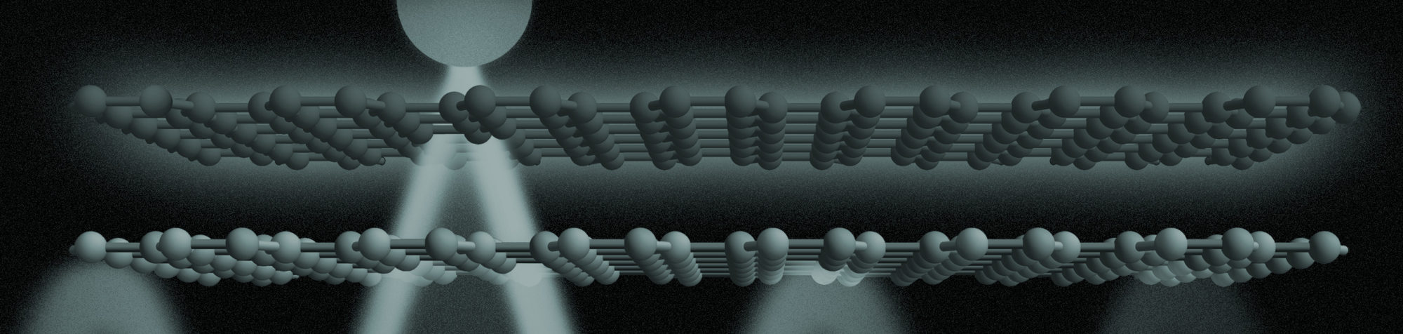
abstract = {Whispering gallery mode (WGM) microdisk resonators are promising optical devices that confine light efficiently and enable enhanced nonlinear optical effects. This work presents a novel approach to reduce sidewall roughness in SiOtextsubscript{2} microdisk resonators using focused ion beam (FIB) polishing. The microdisks, with varying diameter ranging from 5 to 20 μm are fabricated using a multi-step fabrication scheme. However, the etching process introduces significant sidewall roughness, which increases with decreasing microdisk radius, degrading the resonators' quality. To address this issue, a FIB system is employed to polish the sidewalls, using optimized process parameters to minimize Ga ion implantation. White light interferometry measurements reveal a significant reduction in surface roughness from 7 nm to 20 nm for a 5 μm diameter microdisk, leading to a substantial enhancement in the scattering quality factor (Qss) from 3×10^2 to 2×10^6. These findings demonstrate the effectiveness of FIB polishing in improving the quality of microdisk resonators and open up new possibilities for the fabrication of advanced photonic devices.},
keywords = {},
pubstate = {published},
tppubtype = {article}
}
2024
Parul Sharma; Brijesh Kumar; Nihar Ranjan Sahoo; Anshuman Kumar
Exceptional point sensing via energy loss profile in a non-Hermitian system Journal Article
In: Sensors and Actuators A: Physical, vol. 378, pp. 115681, 2024.
@article{arXiv:2310.10111,

title = { Exceptional point sensing via energy loss profile in a non-Hermitian system},

author = {Parul Sharma and Brijesh Kumar and Nihar Ranjan Sahoo and Anshuman Kumar},

url = {https://doi.org/10.1016/j.sna.2024.115681},

doi = {10.1016/j.sna.2024.115681},

year  = {2024},

date = {2024-08-16},

urldate = {2024-08-16},

journal = {Sensors and Actuators A: Physical},

volume = {378},

pages = {115681},

abstract = {The heightened sensitivity observed in non-Hermitian systems at exceptional points (EPs) has garnered significant attention. Typical EP sensor implementations rely on precise measurements of spectra and importantly, for real time sensing measurements, the EP condition ceases to hold as the perturbation increases over time, thereby preventing the use of high sensitivity at the EP point. In this work, we present an new approach to EP sensing which goes beyond these two traditional constraints. Firstly, instead of measuring the spectra, our scheme of EP based sensing is based on the observation of decay length of the optical mode in finite size gratings, which is validated via coupled mode theory as well as full wave electrodynamic simulations. Secondly, for larger perturbation strengths, the EP is spectrally shifted instead of being destroyed — this spectral shift of the EP is calibrated and using this look-up table, we propose continuous real time detection by varying the excitation laser wavelength. As a proof of principle of our technique, we present an application to the sensing of coronavirus particles, which shows unprecedented limit of detection. Furthermore, our analysis includes calculation of the signal-to-noise ratio, revealing that EP sensors offer advantage when classical technical noise dominates over fundamental noise. These findings will contribute to the expanding field of exceptional point based sensing technologies for real time applications beyond spectral measurements.},

keywords = {},

pubstate = {published},

tppubtype = {article}

}
Kishor Kumar Mandal, Anuj Kumar Singh, Brijesh Kumar, Amit P Shah, Rishabh Vij, Amrita Majumder, Janhavi Jayawant Khunte, Venu Gopal Achanta, Anshuman Kumar
Emission engineering in monolithically integrated silicon nitride microring resonators Journal Article
In: ACS Materials Letters, vol. 6, pp. 1831–1840, 2024.
@article{arXiv:2401.04963,

title = {Emission engineering in monolithically integrated silicon nitride microring resonators},

author = {Kishor Kumar Mandal, Anuj Kumar Singh, Brijesh Kumar, Amit P Shah, Rishabh Vij, Amrita Majumder, Janhavi Jayawant Khunte, Venu Gopal Achanta, Anshuman Kumar},

url = {https://doi.org/10.1021/acsmaterialslett.4c00105},

doi = {10.1021/acsmaterialslett.4c00105},

year  = {2024},

date = {2024-04-05},

urldate = {2024-04-05},

journal = {ACS Materials Letters},

volume = {6},

pages = {1831--1840},

abstract = {Monolithic integration of solid-state color centers with photonic elements of the same material is a promising approach to overcome the constraints of fabrication complexity and coupling losses in traditional hybrid integration approaches. A wide band-gap, low-loss silicon nitride (SiN) platform is a mature technology, having CMOS compatibility, widely used in hybrid integrated photonics and optoelectronics. However, it has been shown that certain growth conditions enable the SiN material to host color centers, whose origin is currently under investigation. In this work, we have engineered a novel technique for the efficient coupling of these intrinsic emitters into the whispering gallery modes (WGMs) of the SiN microring cavity -- which has not been explored previously. We have engineered a subwavelength-sized notch into the rim of the SiN microring structure, to optimize the collection efficiency of the cavity-coupled enhanced photoluminescence (PL) spectra at room temperature. The platform presented in this work will enable the development of monolithic integration of color centers with nanophotonic elements for application to quantum photonic technologies.},

keywords = {},

pubstate = {published},

tppubtype = {article}

}
2023
Brijesh Kumar, Anuj Kumar Singh, Kishor K Mandal, Parul Sharma, Nihar Ranjan Sahoo, Anshuman Kumar
A universal and stable metasurface for photonic quasi bound state in continuum coupled with two dimensional semiconductors Journal Article
In: Journal of Physics D: Applied Physics, vol. 56, no. 42, pp. 425105, 2023.
@article{arXiv:2212.05951,

title = {A universal and stable metasurface for photonic quasi bound state in continuum coupled with two dimensional semiconductors},

author = {Brijesh Kumar, Anuj Kumar Singh, Kishor K Mandal, Parul Sharma, Nihar Ranjan Sahoo, Anshuman Kumar},

url = {https://dx.doi.org/10.1088/1361-6463/ace78b},

doi = {10.1088/1361-6463/ace78b},

year  = {2023},

date = {2023-07-27},

urldate = {2023-07-27},

journal = {Journal of Physics D: Applied Physics},

volume = {56},

number = {42},

pages = {425105},

abstract = {The strong coupling of excitons to optical cavity modes is of immense importance when understanding the fundamental physics of quantum electrodynamics at the nanoscale as well as for practical applications in quantum information technologies. There have been several attempts at achieving strong coupling between excitons in two-dimensional semiconductors, such as transition metal dichalcogenides (TMDCs) and photonic quasi-bound states in the continuum (BICs). We identify two gaps in the platforms for achieving strong coupling between TMDC excitons and photonic quasi-BICs: firstly, in the studies so far, different cavity architectures have been employed for coupling to different TMDCs. This would mean that typically, the fabrication process flow for the cavities will need to be modified as one moves from one TMDC to the other, which can limit the technological progress in the field. Secondly, there has been no discussion of the impact of fabrication imperfections in the studies on the strong coupling of these subsystems so far. In this work, we address these two questions by optimizing a cavity with the same architecture, which can couple to the four typical TMDCs (MoS2, WS2, MoSe2, WSe2) and perform a detailed investigation on the fabrication tolerance of the associated photonic quasi-BICs and their impact on strong coupling.},

keywords = {},

pubstate = {published},

tppubtype = {article}

}
Kishor Kumar Mandal; Yashika Gupta; Brijesh Kumar; Mandar Sohoni; Achanta Venu Gopal; Anshuman Kumar
A photonic integrated chip platform for interlayer exciton valley routing Journal Article
In: Journal of Applied Physics, vol. 133, no. 12, pp. 123104, 2023.
@article{doi:10.1063/5.0139880,

title = {A photonic integrated chip platform for interlayer exciton valley routing},

author = {Kishor Kumar Mandal and Yashika Gupta and Brijesh Kumar and Mandar Sohoni and Achanta Venu Gopal and Anshuman Kumar},

url = {https://doi.org/10.1063/5.0139880},

doi = {10.1063/5.0139880},

year  = {2023},

date = {2023-03-30},

urldate = {2023-03-30},

journal = {Journal of Applied Physics},

volume = {133},

number = {12},

pages = {123104},

abstract = {Interlayer excitons in two-dimensional semiconductor heterostructures show suppressed electron–hole overlap resulting in longer radiative lifetimes as compared to intralayer excitons. Such tightly bound interlayer excitons are relevant for important optoelectronic applications, including light storage and quantum communication. Their optical accessibility is, however, limited due to their out-of-plane transition dipole moment. In this work, we design a complementary metal–oxide–semiconductor-compatible photonic integrated chip platform for enhanced near-field coupling of these interlayer excitons with the whispering gallery modes of a microresonator, exploiting the high confinement of light in a small modal volume and high-quality factor of the system. Our platform allows for highly selective emission routing via engineering an asymmetric light transmission that facilitates efficient readout and channeling of the excitonic valley state from such systems.

},

keywords = {},

pubstate = {published},

tppubtype = {article}

}
2022
Lekshmi Eswaramoorthy; Sudha Mokkapati; Anshuman Kumar
Engineering Purcell factor anisotropy for dark and bright excitons in two dimensional semiconductors Journal Article
In: Journal of Physics D: Applied Physics, 2022.
@article{arXiv:2108.10680,

title = {Engineering Purcell factor anisotropy for dark and bright excitons in two dimensional semiconductors},

author = {Lekshmi Eswaramoorthy and Sudha Mokkapati and Anshuman Kumar},

url = {https://doi.org/10.1088/1361-6463/ac570e},

doi = {10.1088/1361-6463/ac570e},

year  = {2022},

date = {2022-02-21},

urldate = {2022-02-21},

journal = {Journal of Physics D: Applied Physics},

abstract = {Tightly bound dark excitons in atomically thin semiconductors can be used for various optoelectronic applications including light storage and quantum communication. Their optical accessibility is however limited due to their out-of-plane transition dipole moment. We thus propose to strengthen the coupling of dark excitons in two dimensional materials with out-of-plane resonant modes of a cavity at room temperature, by engineering the anisotropy in the Purcell factor. A silica micro-disk characterised by high confinement of light in small modal volume, high Q-factor and free spectral range is used to couple to the excitons in monolayer transition metal dichalcogenides. We show numerically that the tapering of sidewalls of the micro-disk is an extremely versatile route for achieving the selective coupling of whispering gallery modes to light emitted from out-of-plane dipoles to the detriment of that from in-plane ones for four representative monolayer transition metal dichalcogenides.},

keywords = {},

pubstate = {published},

tppubtype = {article}

}
2018
Cl'ement Javerzac-Galy*; Anshuman Kumar*; Ryan D. Schilling; Nicolas Piro; Sina Khorasani; Matteo Barbone; Ilya Goykhman; Jacob B. Khurgin; Andrea C. Ferrari; Tobias J Kippenberg
Excitonic emission of monolayer semiconductors near-field coupled to high-Q microresonators Journal Article
In: Nano Letters, vol. 18, no. 5, pp. 3138–3146, 2018.
@article{NL_EPFL,

title = {Excitonic emission of monolayer semiconductors near-field coupled to high-Q microresonators},

author = {Cl{'e}ment Javerzac-Galy* and Anshuman Kumar* and Ryan D. Schilling and Nicolas Piro and Sina Khorasani and Matteo Barbone and Ilya Goykhman and Jacob B. Khurgin and Andrea C. Ferrari and Tobias J Kippenberg},

doi = {10.1021/acs.nanolett.8b00749},

year  = {2018},

date = {2018-04-06},

urldate = {2018-04-06},

journal = {Nano Letters},

volume = {18},

number = {5},

pages = {3138--3146},

abstract = {We present quantum yield measurements of single layer WSe2 (1L-WSe2) integrated with high-Q (Q > 106) optical microdisk cavities, using an efficient (η > 90
keywords = {},

pubstate = {published},

tppubtype = {article}

}
author = {Cl{'e}ment Javerzac-Galy and Nicolas Piro and Ryan D. Schilling and Anshuman Kumar and Matteo Barbone and Ilya Goykhman and Andrea C. Ferrari and Tobias J. Kippenberg},
url = {http://www.osapublishing.org/abstract.cfm?URI=CLEO_SI-2017-STh1I.2},
doi = {10.1364/CLEO_SI.2017.STh1I.2},
year = {2017},
date = {2017-01-01},
urldate = {2017-01-01},
booktitle = {Conference on Lasers and Electro-Optics},
pages = {STh1I.2},
publisher = {Optical Society of America},
organization = {Optical Society of America},
abstract = {We report the functionalization of high-Q silica microdisks with WSe2 and their optical characterization. Background-free cavity enhanced photoluminescence and photoluminescence saturation are observed at room temperature. We show precise measurements of the quantum yield of WSe2.},
keywords = {},
pubstate = {published},
tppubtype = {conference}
}